Article

Strategies towards Cost Reduction in the Manufacture of Printable Perovskite Solar Modules

1
Departamento de Física Aplicada, CINVESTAV-IPN, Mérida 97310, Yucatán, Mexico
2
SPECIFIC IKC, Materials Research Centre, College of Engineering, Bay Campus, Swansea University, Swansea SA1 8EN, UK
*
Authors to whom correspondence should be addressed.
Energies 2022, 15(2), 641; https://doi.org/10.3390/en15020641
Submission received: 10 December 2021 / Revised: 6 January 2022 / Accepted: 11 January 2022 / Published: 17 January 2022
(This article belongs to the Special Issue Thin Films for Energy Applications)

Abstract

:
Among different perovskite solar cell architectures, the carbon-based perovskite solar cell (C-PSC) is a promising candidate for upscaling and commercialization related to low-cost components and simple manufacturing methods. For upscaling a PV technology, three parameters must be considered, corresponding to efficiency, stability, and cost. While the efficiency and lifetime of perovskite technology are the focus of many research groups, the cost parameter is less studied. This work aims to provide information on the manufacturing cost of C-PSC based on experimental data in order to give the readers a panoramic overview of parameters influencing a fabrication process. To analyze the commercialization viability of this technology, we estimated the cost of raw materials and the manufacturing process for sub-modules using two different methods: registration and scribing. The fabrication cost of a sub-module fabricated using the scribing method with 7.9% efficiency was approximately 44% less than that of a device with 6.8% efficiency prepared using registration. We demonstrated that this is due to both the design parameters and performance. In addition, we showed a 51% cost reduction for registration devices by appropriate choice of solar cell components, fabrication steps, and equipment based on the existing infrastructures for the manufacturing of large-scale devices.

1. Introduction

Recently perovskite materials have received significant attention due to their excellent performance in variety of applications such as light emitting diodes (LEDs), resistive memories, X-ray imaging, sensors, catalysis, and photovoltaics [1,2]. The broad absorption spectrum and low nonradiative recombination losses of perovskite materials make them suitable for solar cell applications. The power conversion efficiency of perovskite solar cells (PSCs) has rapidly increased from 3.8% in the first report in 2009 by Miyasaka to 25.2% in 2021, for an aperture area of 0.0804 cm2 [3,4]. One of the key advantages of PSCs is their low-cost manufacturing process related to the low-temperature and solution-based methods using inexpensive and abundant materials [5,6]. Recently, the use of additive manufacturing in solar cell fabrication has shown significant opportunities to establish innovative technologies at a larger size, lighter devices, high throughput processing, and lower manufacturing costs [7,8]. Various steps in the manufacturing process of PSCs are compatible with flexible substrates as well. The fast progress in increasing cell efficiencies whilst decreasing manufacturing cost has motivated researchers around the globe to investigate their potential commercialization.
The main parameters for commercialization viability of a PV technology are efficiency, stability, and cost. Efficiency of PSCs is now exceeding those of multicrystalline silicon, copper indium gallium selenide (CIGS), and cadmium telluride (CdTe) solar cells, which are commercially available PV technologies [9,10].
The long-term stability of perovskite solar cells is still the main barrier for large-scale applications, related to their sensitivity to changes in ambient environments such as humidity, oxygen content, temperature, thermal stress, and UV light [1,11]. Efforts to improve the stability of PSCs include tuning the perovskite structure, device architecture modification, and device encapsulation [12,13,14,15]. An important issue for large-scale applications is the toxicity of lead. Lead-free perovskite solar cells have been reported; however, they are as of yet less efficient and less stable [16,17,18].
When considering cost, this is dependent on the manufacturing approach and choice of materials, which in turn, are dependent on device architecture. There are two main architectures for perovskite solar cells: (i) planar (PPSCs) and (ii) mesoporous (MPSCs) [11,14]. Both devices have shown excellent performance; however, the presence of unstable and expensive hole-transporting materials (HTM) and costly noble metals as counter electrodes increase their manufacturing costs. Han et al. have developed a carbon-based perovskite solar cell (C-PSC) as a fully printable architecture and a promising candidate for large-scale applications related to the easy and cost-effective manufacturing process using stable and abundant materials [19,20,21,22,23]. This innovative architecture can be fabricated without high capital cost equipment, as shown by the production of an A4-sized module using only screen-printing [24] (see a schematic view of screen-printing in Figure S1). Lifetimes of >10,000 h have been reported for this promising technology [15,25].
The C-PSC device consists of a blocking layer, which is usually deposited by spray pyrolysis, and three mesoporous layers (triple stack) of TiO2 as an active layer, ZrO2 or Al2O3 as insulator, and carbon as the counter electrode [19,26]. The perovskite precursor solution is infiltrated through the triple stack to form the perovskite absorber material. The infiltration and conversion processes can be carried out via a one-step or two-step deposition method [27,28]. In the two-step (sequential) method, a solution of lead iodide (PbI2) in DMF is drop-casted onto the carbon layer, and after drying and solvent evaporation, the stack is immersed into a solution of methylammonium iodide (MAI) in isopropyl alcohol (IPA) for a couple of minutes to form the perovskite. In the one-step deposition method, both perovskite infiltration and conversion take place in one step, using a mixture of PbI2 and MAI in an organic solvent such as gamma-butyrolactone (GBL), dimethyl sulfoxide (DMSO), a mixture of DMSO and dimethylformamide (DMF) and, n-methyl-2-pyrrolidone (NMP) [29,30,31,32]. The choice of one-step or two-step perovskite deposition method affects the properties of the perovskite layer. It is reported in the literature that high-quality crystalline perovskite can be obtained from the two-step method. The perovskite morphology obtained from the sequential technique shows larger grain size and less grain boundaries, resulting in better photovoltaic performance and reproducibility.
On the contrary, the one-step deposition technique may result in incomplete conversion, smaller degree of perovskite coverage, and non-homogeneous particle size of the perovskite grains. However, the two-step deposition method is suitable for fabrication in the laboratory and achieving high performance, while the one-step method is ideal for the fabrication of large-scale devices, as will be explained later [33,34].
To achieve high-efficiency and reproducible devices, experimental parameters such as layer thickness, type of solvent, solution composition, concentration and temperature, infiltration drop volume, annealing temperature, and conversion time need to be optimized [35,36,37,38,39]. Up to now the power conversion efficiency (PCE) of the triple stack devices has been between 10% and 16% for cells with a small active area up to 1 cm2 [38,40,41,42,43,44].
There are only a few reports on the scale-up of the C-PSCs to larger devices. Hu et al. fabricated a monolithic module with a large area of 10 × 10 cm2, which consisted of 10 serially connected sub-cells with a total active area of 49 cm2. The module achieved an efficiency of 10.40% and one year indoor stability for an unsealed module in the dark, and one month outdoor stability of the encapsulated module under local environment in China [45]. Priyadarshi et al. modified the module design and active area, and examined the performance of three different carbon pastes to achieve the lowest electrical resistance and the highest perovskite filling fraction of the TiO2 and ZrO2 by modification of the carbon particle size. They also used a 100-cm2 area substrate (device area) to fabricate a monolithic module with 10 connected cells in series, and total active area of 70 cm2. They obtained an efficiency of 10.75% and ambient stability of more than 2000 h [46]. De Rossi et al. reported the fabrication process of a device using the registration of the overlapping layers with 198 cm2 of active area and an average PCE of 6%. They studied the effect of patterning the TiO2 blocking layer to improve the interconnection between adjacent cells, resulting in lowering the contact resistance and improving the fill factor and module performance. For future increase in the module efficiency, they proposed a humidity post-treatment in the dark and obtained over two months of stability for unencapsulated devices [24]. In recent work of Meroni et al., the manufacture and performance of a 10 × 10-cm2 device using the so-called mechanical scribing method is reported addressing a systematic study of the interconnection area between adjacent cells. A geometrical fill factor of 90% and a module efficiency of 10.37% were obtained showing that a critical element in achieving appropriate interconnects is the contact resistance at the FTO/carbon interface [47].
Related to the limited extent of scale-up efforts, to our knowledge there are no reports on the manufacturing cost of large-area perovskite devices based on experimental data. For an appropriate cost estimation for the viability of a solar project, the choice of PV module architecture, raw materials and components, and manufacturing steps are very important to reduce the levelized cost of energy (LCOE) value.
In this paper, we propose two different configurations for carbon-based perovskite solar modules, and we discuss how the manufacturing cost can be reduced by an accurate choice of raw materials and fabrication steps considering different fabrication strategies. The cost per kWh for each proposed strategy is calculated using experimental data in order to obtain a comparison of the manufacturing cost of a solar module. The LCOE calculation is beyond the scope of this paper; however, the proposed optimum module architecture and manufacturing process in this paper will be the starting point for the cost estimation and feasibility study of economics and facilities for production of printed photovoltaics.

2. Materials and Methods

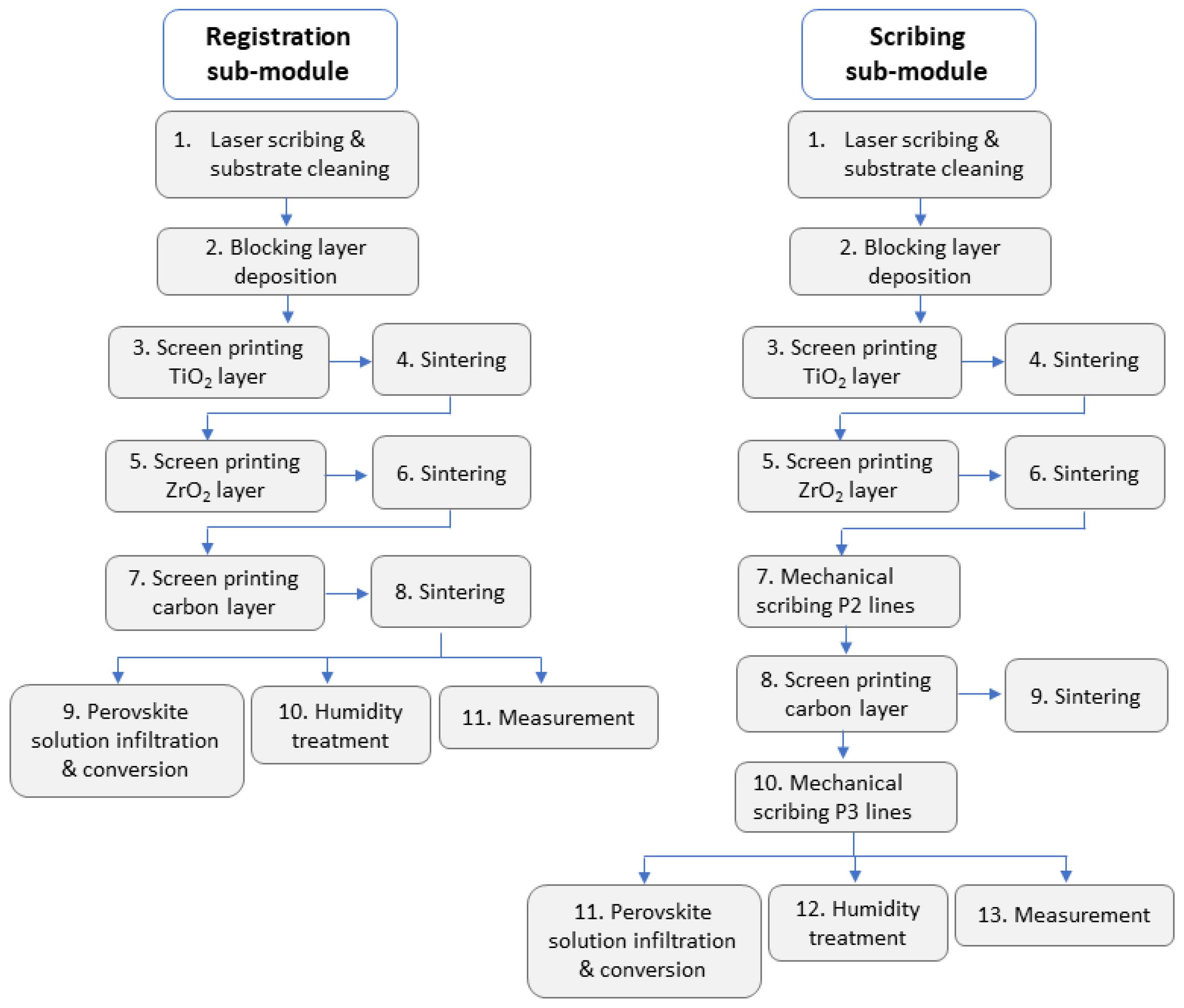
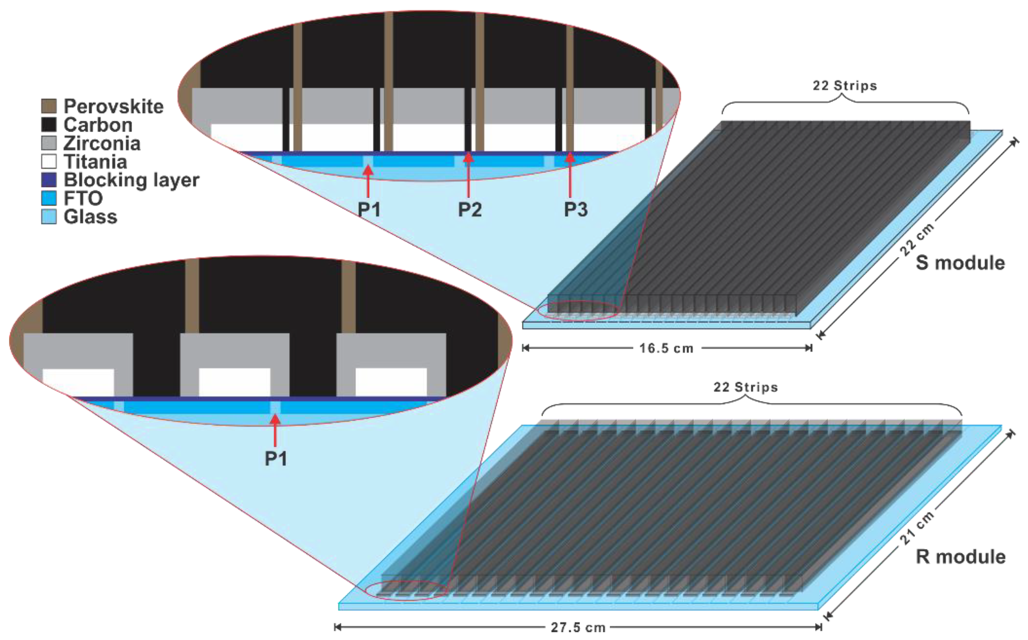
2.1. Solar Module Manufacturing Process

Two modules with different design parameters were fabricated. The fabrication steps are presented in Figure 1 for both devices. One was manufactured using the registration method (R module) where the overlaying of layers is required for interconnection; this is achieved using printing accuracy instead of material removal. The second module was fabricated using the scribing method (S module). In this method, the interconnections are created based on a material removal approach to achieve a high geometrical fill factor (ratio between the active area and total area).
The details of the manufacturing process have been reported previously [24,47]. First, the P1 isolating line was scribed on the FTO substrate using an Nd:YVO4 laser. The substrate (XOP Glass) size was 27.5 × 21 and 22 × 16.5 cm2 for R and S modules, respectively. The substrate cleaning, blocking layer deposition, triple stack screen-printing, and the annealing processes were carried out using the same procedures as for the small solar cells described in supplementary materials [41]. The final thickness of the mesoporous TiO2, ZrO2, and carbon films was 0.8, 1.2, and 12 µm, respectively, and all three layers were printed from commercially available pastes. For the S module, the P2 and P3 scribes were applied mechanically using a steel blade. For more details see reference [47]. The AVA-MAPI precursor solution was prepared with 439 mg of PbI2, 151.4 mg of MAI, and 6.7 mg of 5-AVAI in 1 mL of GBL. A so-called robotic mesh (RbM) method was used to spread the precursor solution on the surface of the triple stack [41]. The wet devices were kept in a closed petri dish for 10 min at room temperature and then heated at 50 °C in an oven for 2 h. Then the modules were treated at 70% RH inside the humidity oven at 25 °C for 24 h. Figure 2 shows the schematic views of the R and S modules, and Table S1 in the supplementary materials shows the design parameters for each module. Both modules are fabricated on FTO substrates and consist of 22 large cells that include a blocking layer, and titania, zirconia, and carbon layers.
For both modules, first, the P1 line was scribed onto the FTO substrate using a laser machine to remove the transparent conductive layer from the substrate. Then, titania and zirconia layers were screen-printed. For module R, accurate registration is necessary to print the titania layer above and close to the P1 line without contacting it. The zirconia layer is printed on the top of the titania layer to cover it, and it should also cover the P1 line. For module S, titania and zirconia layers are printed on the entire substrates, and then the P2 line is mechanically scribed to remove the unwanted areas. The carbon layer is printed on the top of the two previous layers. In module R, care must be taken to print the carbon layer in such a way as to avoid any contact with the adjacent carbon layer from the neighbouring cell. In the scribing module, the carbon is printed on the top of two other layers and the unwanted areas are removed by applying P3 lines mechanically.

2.2. Cost Analysis: Solar Module Manufacturing Process

The cost analysis and manufacturing cost calculations are based on a bottom-up strategy. It means that the cost of each raw material and electricity consumption of each process, which are required to fabricate the registration (R) and scribing (S) modules, was calculated. This calculation is based on the quantity and cost of raw materials used in the structure of each module, as well as the duration of each fabrication process and electricity price (see Tables S2–S5). To estimate the fabrication cost of sub-modules based on cost reduction strategies, different configurations were investigated for each type of module, i.e., R1 to R6 and S1 and S2, assuming the following innovations. The R1 sub-module is considered to be the most expensive device consisting of the use of commercially available pastes, the two-step perovskite deposition method, and three conventional heat treatments in a furnace. The R2 sub-module has the same configuration as the R1 device; however, the one-step method for perovskite deposition was implemented. To reduce the fabrication cost in the R3 device, the use of low-cost pastes was proposed [48,49]. In the R4 sub-module, low-cost pastes and one-step perovskite deposition were assumed. In addition, to reduce the manufacturing cost, two heat treatments after zirconia and carbon layer deposition were considered instead of three heat treatments. For the R5 device, all three conventional heat treatments were replaced with an NIR treatment. The R6 sub-module is considered to be the most cost-effective device among the R-series devices. This sub-module consists of the triple stack prepared from low-cost pastes, one-step perovskite deposition, NIR treatment, and production under ambient atmosphere instead of dry room facilities, as the steps considered for the fabrication. For the S-series sub-module, the S1 device was prepared with commercially available pastes, one-step perovskite deposition, and three conventional heat treatments. The S2 device is a cost-effective configuration fabricated with low-cost pastes, one-step perovskite deposition, NIR treatments, and ambient atmosphere.
In this case, we considered the cost of raw materials, components, and equipment electricity consumption for the different manufacturing steps. The results of the cost analysis show which component or process step has the largest cost contribution in the manufacturing process of a triple stack module. Strategies to reduce the final cost were proposed, and an optimum module design to achieve an improvement in the performance and decrease of the cost was presented. In addition, the manufacturing cost per Watt·hour was calculated to determine a cost-effective strategy for the future module production line.

3. Results

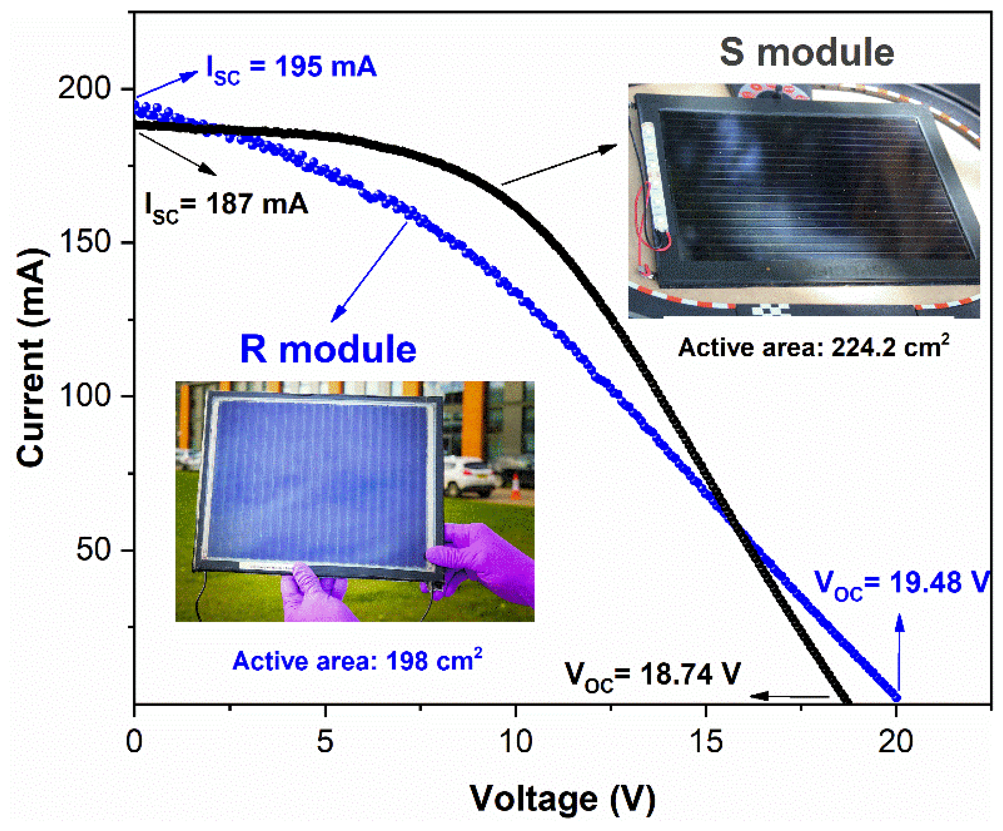
3.1. Module Performance
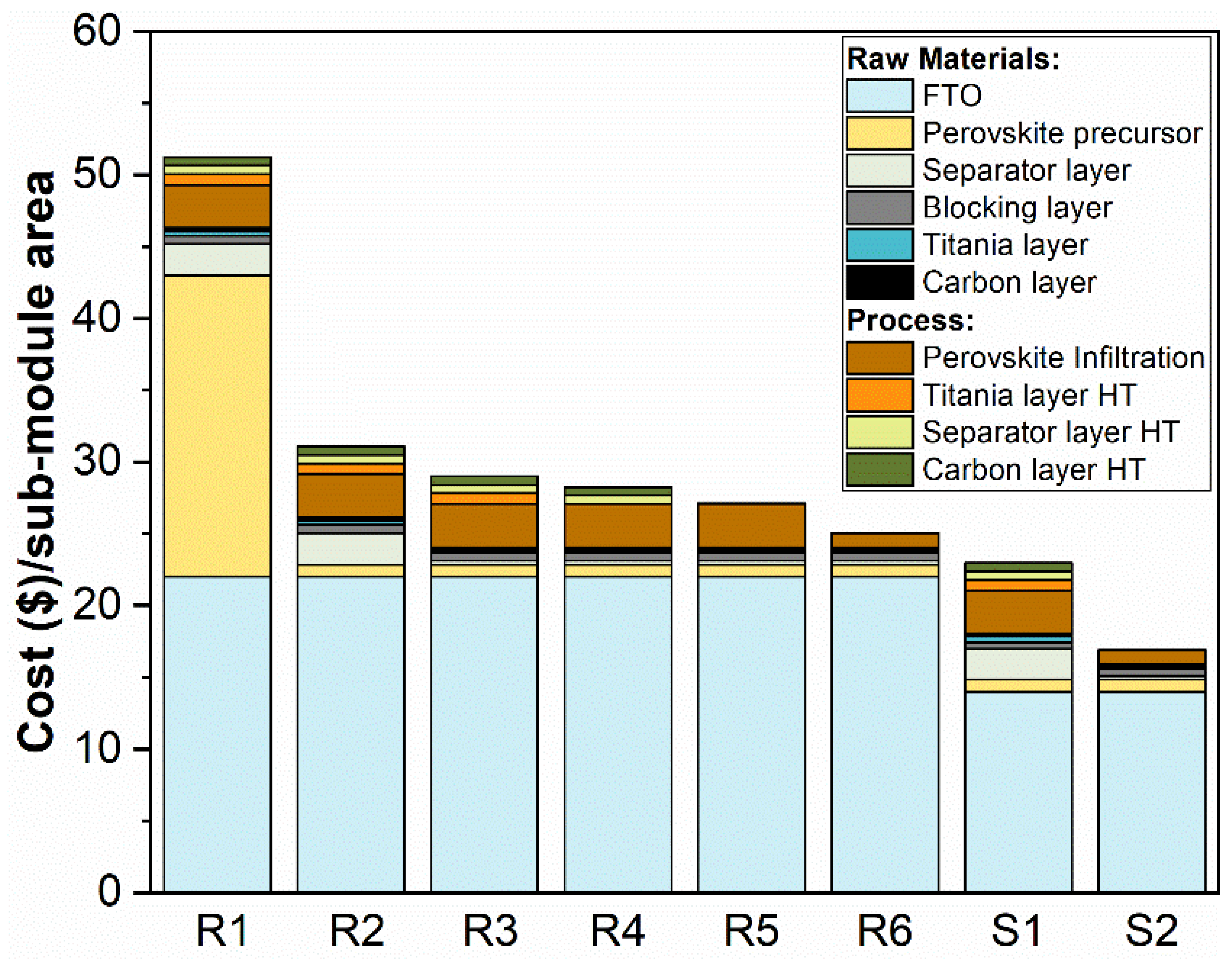
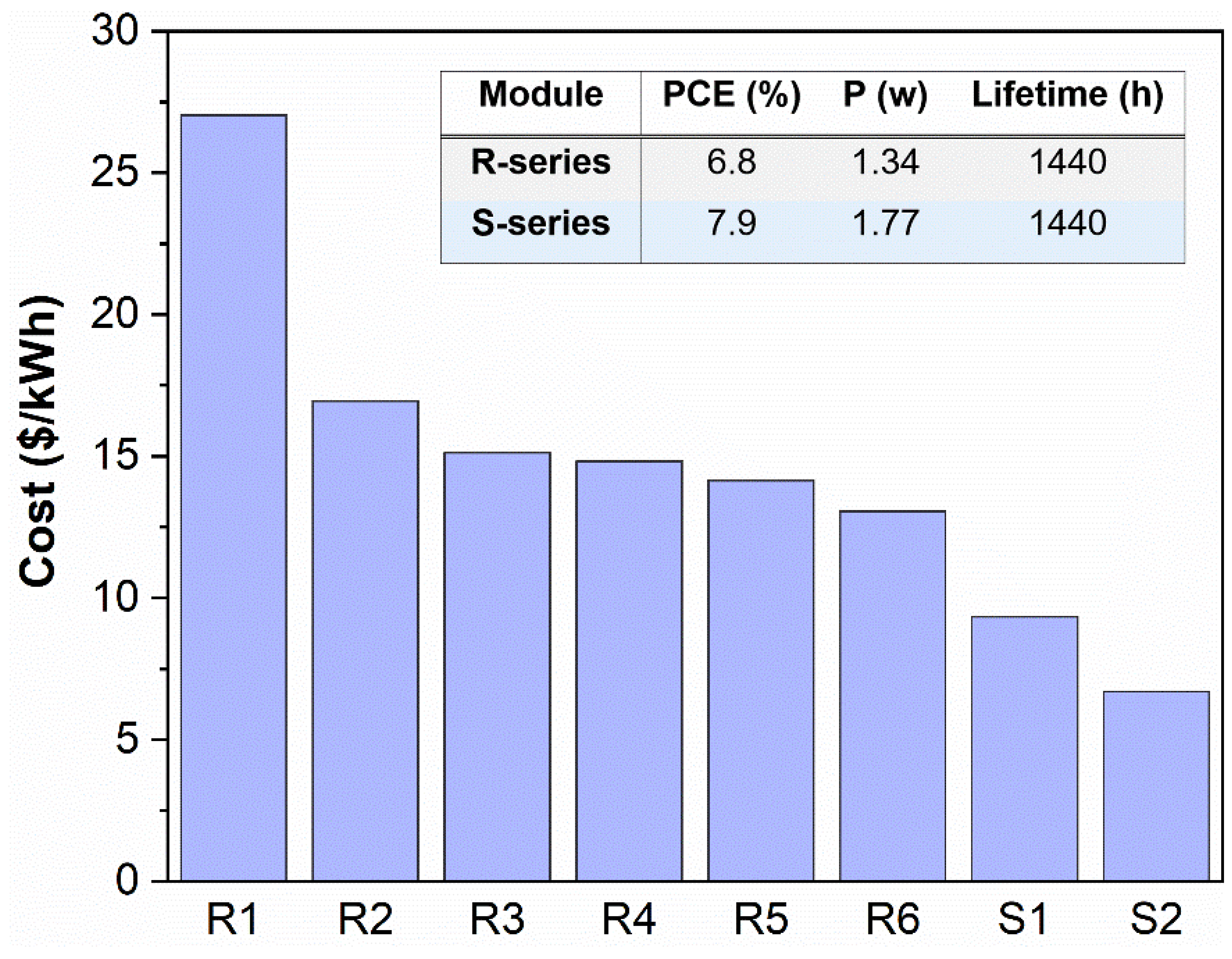
Figure 3 shows the IV curves for the R and S modules. The photovoltaic performance parameters are listed in Table 1. Although the R module has a higher current density and open circuit voltage; its fill factor and thus the power conversion efficiency are lower than those of the S module. For the R module, the interconnections were created using an accurate registration of each layer via the screen-printing technique. A margin was considered to prevent possible shunts; however, this resulted in increasing the total un-used area and, hence, decreases the geometrical fill factor. In the S module, the Ohmic losses through the carbon electrode were minimized using narrow scribing lines which ensure sufficient interconnection area between adjacent cells and result in an improvement in module fill factor and efficiency.

3.2. Module Cost

Here, we calculated the fabrication cost of a module based on the existing laboratory infrastructure, and we proposed various strategies to reduce the device cost by replacing raw materials and modifying the module design. The difference among R-series modules (from R1 to R6 in Figure 4) is in the replacement of low-cost raw materials and/or changing the fabrication process (one-step perovskite deposition vs. two-step technique). Both strategies result in a reduction in cost and quantity of required materials. The difference between R and S modules is the module’s design. By changing the design, a smaller conductive glass substrate was used for the S module. The conductive glass substrate has the largest contribution in cost of raw materials according to our calculations (see Tables S2 and S4). Therefore, by changing the design parameters, a lower quantity of raw materials was needed, which directly led to a reduction in the materials’ cost.
Table S2 in the supplementary materials shows the R module components, their purchasing price ($/kg), and the required quantity of each component for module manufacturing (kg). Table S3 shows the processes used in module manufacturing and the corresponding electricity consumption. The manufacturing costs in US dollars ($) were calculated using these two tables and are shown in Figure 4, where the contribution of each component and process in the cost of module manufacture is presented. Each module in this figure represents a new strategy to reduce the manufacturing cost. Note that the cost of raw materials such as cleaning agents and Sn wire, and processes such as humidity treatment, blocking layer deposition, triple stack screen-printing, patterning by laser, substrate cleaning, and soldering were considered in our calculations (see Tables S2–S5); however, as these values were negligible, they are not shown in Figure 4. For R-series modules, the fabrication method was registration and for S-series modules the mechanical scribing method was used. For both configurations, the FTO glass had the highest cost contribution as compared to the other components. Module R1 was fabricated using the commercially available pastes of titania, zirconia, and carbon, and the two-step perovskite deposition technique in which the solution of PbI2 in DMF was infiltrated into the triple stack. After annealing, the substrate was immersed into the solution of MAI in anhydrous IPA. This method is commonly used for small-scale cell fabrication. There are several reports in literature that consider the MAI dip coating step for large-scale applications [21,50]. However, the viability of this method for large-scale manufacturing is questionable due to the large amount of raw materials required and the generation of significant residues.
The best alternative to the two-step method is a one-step deposition method, in which an exact quantity of the perovskite precursor solution is infiltrated into the triple stack with the minimum waste of raw materials and almost no residue production. A one-step deposition technique is a material and time saving strategy, and allows for a continuous production process. This can be achieved with the robotic mesh (RbM) method that has been previously reported, which provides homogeneous and effective deposition of the perovskite solution onto the stack [47]. In Figure 4, it can be observed that the R1 module using the two-step perovskite deposition method is $20 more expensive than the R2 module in which the one-step perovskite deposition method is used. Besides the reduction in raw materials quantity and therefore costs, another advantage of the one-step deposition method is its compatibility with other processes in a large-scale production line. It means that after sintering the triple stack, the large module is transferred directly to the next step, which is the RbM one-step infiltration. This strategy matches with a continuous process for large volume production, whereas the two-step deposition technique could be useful for a batch process and low volumes. Applying the one-step deposition technique could decrease the overall production time and increase the production rate (m2/min), which directly influence the total manufacturing costs.
To further decrease the manufacturing costs, commercially available pastes in the R2 module design were replaced with low-cost, home-made titania, and alumina pastes, corresponding to the R3 module. The nanomaterial synthesis, paste preparation, and paste cost analysis are explained in detail in the supplementary materials. The cost of commercial titania and alumina pastes in the R2 module was 9.6% of the total raw materials costs, while for prepared titania and alumina pastes in the R3 module this was only 1.7%. In the R-series modules, the TiO2 printed area was 198 cm2 and the ZrO2 printed area was 327 cm2 (see Table S1). The cost difference between the prepared pastes and commercially available pastes increases for larger scale devices, where the printed area and therefore the amount of required pastes is larger.
Although the carbon-based perovskite devices have shown potential for scale-up, one barrier for large-scale application is the sintering processes in their manufacturing. Usually after each mesoporous layer deposition, the layers are thermally treated for several hours to remove any organic binders of the pastes and to improve the interconnection between nanoparticles. The sintering is costly due to the electricity consumption of conventional furnaces, and it is time consuming, which reduces the production rate. One strategy to overcome this barrier is to decrease the number of sintering steps. Figure 4 illustrates that the sintering processes of titania, zirconia, and carbon have a high contribution in electricity consumption cost, corresponding to about 37% of the total cost of electricity for the manufacturing processes of R1, R2, and R3 modules.
Since both titania and zirconia are metal oxides, the process may be simplified by sintering both layers in one step. In this case, after screen-printing of the titania layer, it was allowed to dry for several minutes before starting the screen-printing of the zirconia layer. Both layers were then sintered in one step at a high temperature in the furnace. It may even be possible to sinter all three mesoporous layers at the same time; however, because of the different nature of the carbon layer, this possibility needs to be carefully evaluated in relation with the performance of the device. Here, we only considered the possibility of two sintering steps in R4 module instead of the three sintering steps in R3. For the R4 module, the electricity consumption related to the two sintering steps was around 29% of the total electricity consumed in all the other processes: decreasing the number of heat treatment steps from 3 to 2 resulted in approximately 11% reduction in total electricity consumption cost of the manufacturing process.
Another strategy for lowering the costs related to sintering is to modify the process using near-infrared (NIR) treatment as reported previously [42]. In the R5 module, after each screen-printing step, the mesoporous layer was left to dry for 5 min and the NIR treatment was applied for 60 s. The total electricity consumption cost decreases by approximately 36% compared with the three sintering steps in a conventional furnace. Another important advantage of this method was a lowering of the processing time, which may result in a significant increase in the production rate. The duration of processes such as cleaning, screen-printing, and spray pyrolysis was almost negligible compared to the heat treatment and annealing processes. If we consider the sintering of a triple stack as a time-dominant process in the fabrication of R modules with 198 cm2 total active area, then the production rate would be 0.5 and 11 cm2/min by conventional furnace and NIR treatment, respectively. Hence, by using the NIR treatment, the manufacturing rate is about 22 times faster compared with the conventional 3 steps heat treatment. This strongly influences the techno-economic aspect of a large-scale production line where the manufacturing cost depends significantly on the production rate.
Other costly processes in the fabrication of perovskite solar devices are the perovskite precursor solution preparation and perovskite deposition process. For small solar cells and mini modules, these steps are usually carried out in a dry room where the relative humidity can be controlled using a dehumidifier. However, for large-scale applications, these steps should be carried out in an ambient atmosphere to reduce the electricity consumption corresponding to humidity control. The R6 module shows the cost of an R type module fabricated with the low-cost titania and alumina pastes, one-step perovskite deposition, NIR treatment as sintering step, and infiltration under ambient atmosphere conditions. Using these processes, the electricity consumption cost decreases approximately 75% compared with for the R2 module in which the conventional processes have been used.
Finally, the design parameters of the R module were modified to: (1) decrease the use of the FTO substrate, which has the highest contribution in cost of raw materials, and (2) increase the total active area and, hence, module efficiency. In this case, the total device area was decreased from 577.5 cm2 in the R module design to 363 cm2 in the S module design, while the number of the small cells (22 cells) did not change (see Table S1). The cost per unit area of device is reduced from $51.75 to $25.5 from R1 to R6 and from $23.5 to $18 from S1 to S2.
The cost of raw materials ($/kg) and the fabrication processes for an S module are listed in Tables S4 and S5, respectively. Due to the precision scribing of the P2 and P3 lines, the active area of the S module of 224.2 cm2 is significantly larger than for the R module, where the active area is 198 cm2. Therefore, the total active area for the S module was 61.7% of the total device area, compared to 34.3% for the module R. In Figure 4 the fabrication cost of module S1 is compared with the manufacturing cost of module R2, in which the same raw materials and fabrication steps were used. The final manufacturing cost decreased by about 27%, changing from the R module design to the S module configuration. In module S2, the manufacturing cost could be decreased even further by using the low-cost pastes and the fast NIR heat treatment under ambient conditions.
In Figure 4, the total manufacturing cost of different modules was shown without considering their photovoltaic performance. In the cost reduction scheme we presented in this work, we showed that the manufacturing cost can be reduced by choice of low-cost pastes, adequate equipment, and proper design parameters. These strategies are reflected in all modules presented, from R1 to S2. The S2 module represents the optimum module design and a choice of the most adequate raw materials and processes. For a fair comparison of modules cost, and to show the effect of the solar energy conversion efficiency and device lifetime on the total manufacturing cost of each module, the cost per kWh was calculated, which is presented in Figure 5. The reported efficiencies in Table 1 correspond to the R2 and S1 modules, which were fabricated in the laboratory. For this reason, in the following lines, we focus on the comparison between these two modules. In addition, a lifetime of 1440 h was reported for these modules [24]. These parameters, based on experimental data for R2 and S1 modules, are shown in the inset of Figure 5. Although the other modules (R1, R3, R4, R5, R6, and S2) were not fabricated and are “simulated devices” representing the effects of cost reduction strategies, the same parameters for the efficiency and lifetime were assumed.
The total manufacturing cost decreased from 16.4 to 9.2 $/kWh by changing the design parameters of the R2 module to the S1 module. The approximate 44% cost reduction was due to the decrease in the amount of raw materials used, such as FTO and printed zirconia and carbon, as well as an improvement in module active area and, hence, efficiency and output power. The manufacturing cost can be decreased to US $7 per kWh by replacing the sintering processes in a conventional furnace by the fast NIR heat treatment. As is well known, to evaluate the commercial feasibility of a new PV technology, the levelized cost of electricity or energy (LCOE) of a solar power plant based on that PV technology is calculated and compared with the LCOE of the commercially available PV technologies. The LCOE is the total cost of building an electricity generating plant over the total energy produced by the plant during its lifetime. According to this definition, a feasible PV technology for commercialization must meet a low capital cost, high efficiency, and long lifetime. The first and second-generation solar cells have already reached a very low LCOE, which makes it quite difficult for the perovskite community to compete. Although the capital cost for the manufacturing of the first and second-generation solar panels has significantly decreased in recent years, the low LCOE is mostly due to the high efficiency (>15%) and long lifetime (25–30 years). To our knowledge, in the literature, for an accurate comparison between the cost of the perovskite PV technology and the commercially available solar panels, the efficiency of 15 to 20% and lifetime of 15 to 30 years are assumed to calculate the LCOE [5,10,21,49]. This assumption is due to the lack of the experimental data for the perovskite PVs. It should be mentioned that the cost per kWh in this paper was based on the experimental efficiency of ≈7 and 8% and lifetime of 1440 h. For the S2 module, with the lowest manufacturing cost and the highest experimental efficiency, if we assumed an efficiency of 15% and a lifetime of 15 years (131,400 h), the cost per kWh would be ≈0.041 $/kWh, which is comparable with the cost of the commercially available PV technologies (32–44 $/MWh) [51]. It is worth mentioning that in this paper the module manufacturing cost was calculated based on the existing infrastructure in the laboratory using the cost of raw materials in batch. For a future commercialization, the high cost related to the use of small batches would be reduced significantly by purchasing the raw materials in bulk, which results in a further decrease in cost per kWh of perovskite PV.
Therefore, several advantages such as the ease of perovskite PV manufacturing, low capital cost, compatibility with the flexible substrates (suitable for the roll-to-roll process), high open circuit voltage and therefore device functionality under low-light intensity (suitable for indoor and internet of things (IOT) applications), and the stability of the triple stack architecture are the main motivations for the perovskite community to improve the device efficiency and stability to compete with the commercially available PV technologies.

3.3. Future Directions

In this work, we estimated the manufacturing cost of carbon-based perovskite C-PSC solar modules in the laboratory with the available infrastructure and based on experimental performance data. We calculated the manufacturing cost using the purchasing price of raw materials in partial quantities. As a result, the most expensive component for module fabrication was the FTO transparent conducting glass substrate, while the cost and production time that dominate the fabrication process corresponds to the conventional thermal treatment of the triple stack. Usually, for the viability study of a PV technology, a large-scale production line with the capital cost for purchasing the manufacturing equipment and raw materials in bulk are considered. For example, to produce conductive substrates for large devices, glass substrates are purchased at a bulk price and a sputtering set-up is installed to deposit the conductive transparent layer [10,48,49]. As we showed, the second most expensive component of the C-PSC is the separator layer due to the high cost of zirconia or alumina paste and the required quantity of this material for large devices. For a future production line, an extra unit for paste production can be considered in order to reduce the cost of this component as partial purchasing, especially for the countries that must pay a high importation cost for the imported products. Hence, the cost of extra equipment, facilities, utilities, and labor for the material manufacturing synthesis and paste preparation should be considered. In a production line of large-scale devices, all manufacturing steps should be compatible and match with a continuous flow process to avoid a slow production rate and, hence, higher manufacturing cost. One example is the two-step deposition technique which results in: (1) a high volume of raw materials and residues for the MAI conversion process by immersion, and (2) a disconnect in the production line in order to place the large substrate inside the immersion bath. On the other hand, using a one-step deposition technique is a material and time saving strategy, and allows for a continuous production process. For an appropriate cost estimation of a production line, a trade-off between the capital cost and process effectiveness (in cost, time, and performance) should be considered. For example, for R and S modules, most of the fabrication equipment and facilities are the same. The scribing line in the R module can be applied using a low-cost laser machine; however, the P2 and P3 lines in S modules are scribed using more sophisticated and high-cost laser systems. This may increase the capital cost for production of S modules compared to that of R modules. However, analysis of the drawbacks of the R module leads to choosing for a production line with a slightly higher capital cost, but less labor cost and better device performance. The disadvantages of the R module design are: (1) an extra expert labor cost is required for the registration printing process where high accuracy is needed in order to print the layers in their exact positions; (2) reduction in the production rate due to the semi-automatic printing steps with labor supervision; and (3) decrease in quality and device performance. On the contrary, the S module can be fabricated in a continuous process using a highly accurate laser scribing system and higher production rate.
Finally, we have shown that the sintering process in the fabrication of the carbon PSC devices is costly and time consuming. If this step is replaced by an NIR heat treatment, the capital cost may increase; however, the production rate also increases. It means that a larger area (m2) and more devices can be produced during an assumed operation time. This directly influences the $/kWh cost of a module. The choice of the right module configuration and manufacturing process parameters is a key factor for a future design of a carbon PSC module production line. The extensive cost estimation of a large-scale module production line, including the capital, labor and utilities costs, equipment maintenance and depreciation, land, taxes, etc., will be discussed in future work using the optimum module design proposed in this work.

4. Conclusions

In this work, the manufacturing cost of large C-PSC devices was calculated, showing that the FTO substrate is the most expensive raw material and that the sintering process is the most critical factor influencing the cost and production rate. The cost of the separator layer as the second most expensive raw material, can be decreased by a factor of 7.7 using the home-made paste. This can be observed in Figure 4 by the change in height of the bright gray box from the R2 to R3 module configuration, which represents the cost of the separator layer. The results of solar cells performance and reproducibility (see the supplementary materials) show that the pastes developed in this work can be considered as viable low-cost alternatives for large-scale applications. We have shown that the cost per kWh of a module decreases significantly by improving the module efficiency. The cost estimation of the manufacturing process has shown that: (i) the two-step perovskite deposition technique must be replaced by one-step deposition technique; (ii) the registration method for module fabrication should be replaced by scribing method, and (iii) the sintering processes must be conducted in less steps or completely replaced by fast heat treatment methods. We showed an approximately 51% cost reduction for registration devices (from R1 to R6) by appropriate choice of solar cell components, fabrication steps, and equipment based on the existing infrastructures for the manufacturing of large-scale devices. In addition, by applying all these strategies, a 75% reduction in module manufacturing cost could be achieved (from R1 to S2 configuration).
To determine the commercial viability of carbon-based perovskite photovoltaic technology and lab-to-fab transition, the costs of an operating plant with different manufacturing units including capital costs, facilities, wages, and overheads must be determined based on the right choice of materials and process. As commercial viability strongly depends on the efficiency and lifetime of the PV device, extensive research should continue to increase the conversion efficiency and improve the stability of large-scale devices.

Supplementary Materials

The following supporting information can be downloaded at: https://www.mdpi.com/article/10.3390/en15020641/s1, Figure S1: Schematic of the screen-printing method; Table S1: Design parameters for R and S modules; Table S2: Raw materials and components and their corresponding price/kg and the cost of required quantities for the fabrication of the A4 size R module; Table S3: Processes and the corresponding costs for the fabrication of the R module; Table S4: Raw materials and components and their corresponding price/kg and the cost of required quantities for the fabrication of the S module; Table S5: Processes and the corresponding costs for the fabrication of the S module; Figure S2: (a) X-ray diffraction pattern of TiO2 powder synthesized in this work; the inset shows the corresponding SEM image; (b) X-ray diffraction pattern of the Al2O3 material synthesized with the SEM image of the alumina powder in the inset; Table S6: The cost comparison between the pastes prepared in this work and commercially available pastes for 1 kg of the final product, for availability in Mexico; Figure S3: (a) Cost comparison of the prepared pastes and the commercially available pastes; (b,c) Cost breakdown for the titania and alumina pastes, respectively; Figure S4: Box chart of photovoltaic parameters of three series of devices compared to the standard device: Std device: triple stack of commercial pastes; Device A: home-made titania and commercial zirconia and carbon, Device B, home-made alumina and commercial titania and carbon; Device C: home-made titania and alumina and commercial carbon; Figure S5: Titania layer deposited on the glass/FTO substrate from: (a) GreatCell Solar titania paste; (b) CINVESTAV paste; Table S7: Triple stack composition and the final films thickness for four series of fabricated devices as standard (Std), A-, B-, and C-series devices; Table S8: Photovoltaic parameters for fabricated cells with different pastes.

Author Contributions

Funding acquisition and resources: A.W., G.O. and T.W. Scientific guidance: G.O. and T.W. Solar cell fabrication, data acquisition, and writing the manuscript: D.P. Module fabrication and data acquisition: S.M.P.M. The principal idea and scientific guidance: J.B. Alumina synthesis and paste preparation: A.S.M. and D.P.D. Graphs and schematic designs: R.E. All the authors have worked on the abstract and conclusions. All authors have read and agreed to the published version of the manuscript.

Funding

This research was funded by CONACYT-SENER, and the NEWTON FUND of the British Council for the financial support under grant number “FSE-291504”, the GLOBAL RESEARCH TRANSLATION AWARD through the project “Power to the people: Democratising energy through decentralised manufacture and production of affordable, reliable, sustainable solar power”, “EGR 1295”, the ROYAL SOCIETY INTERNATIONAL COLLABORATION AWARD, “ ICA\R1\191321”; the NEWTON FUND IMPACT SCHEME “541128962”, and CONACYT under the FORDECYT-PRONACES project “318703”. Also, this work was made possible by support from the UKRI Global Challenge Research Fund project SUNRISE (EP/P032591/1).

Acknowledgments

We would like to acknowledge Dora Huerta and Daniel Aguilar for technical assistance supported by the Laboratorio Nacional de Nano y Biomateriales (LANNBIO)-CINVESTAV-Mérida.

Conflicts of Interest

The authors declare no conflict of interest.

References

  1. Huang, F.; Li, M.; Siffalovic, P. From scalable solution fabrication of perovskite films towards commercialization of solar cells. Environ. Sci. 2018, 12, 518–549. [Google Scholar] [CrossRef]
  2. Park, N.-G. Halide perovskite photovoltaics: History, progress, and perspectives. MRS Bull. 2018, 43, 527–533. [Google Scholar] [CrossRef] [Green Version]
  3. Kojima, A.; Teshima, K.; Shirai, Y.; Miyasaka, T. Organometal halide perovskites as visible-light sensitizers for photovoltaic cells. J. Am. Chem. Soc. 2009, 131, 6050–6051. [Google Scholar] [CrossRef] [PubMed]
  4. Jeong, J.; Kim, M.; Seo, J.; Lu, H.; Ahlawat, P.; Mishra, A.; Yang, Y.; Hope, M.A.; Eickemeyer, F.T.; Kim, M.; et al. Pseudo-halide anion engineering for α-FAPbI3 perovskite solar cells. Nature 2021, 592, 381–385. [Google Scholar] [CrossRef]
  5. Chang, N.L.; Ho-Baillie, A.W.Y.; Vak, D.; Gao, M.; Green, M.A.; Egan, R.J. Manufacturing cost and market potential analysis of demonstrated roll-to-roll perovskite photovoltaic cell processes. Sol. Energy Mater. Sol. Cells 2018, 174, 314–324. [Google Scholar] [CrossRef]
  6. Ahmed, M.I.; Habib, A.; Javaid, S.S. Perovskite Solar Cells: Potentials, Challenges, and Opportunities. Int. J. Photoenergy 2015, 2015, 1–13. [Google Scholar] [CrossRef] [Green Version]
  7. Mehta, V.R.; Ravindra, N.M. Screen Printing to 3D Printing of Solar Cells—An Overview. In Proceedings of the TMS 2020 149th Annual Meeting & Exhibition, San Diego, CA, USA, 23–27 February 2020; pp. 1935–1944. [Google Scholar]
  8. Khorasani, M.; Ghasemi, A.; Rolfe, B.; Gibson, I. Additive manufacturing a powerful tool for the aerospace industry. Rapid Prototyp. J. 2022, 28, 87–100. [Google Scholar] [CrossRef]
  9. Green, M.A.; Dunlop, E.D.; Hohl-Ebinger, J.; Yoshita, M.; Kopidakis, N.; Hao, X. Solar cell efficiency tables (version 59). Prog. Photovolt. Res. Appl. 2022, 30, 3–12. [Google Scholar] [CrossRef]
  10. Song, Z.; McElvany, C.L.; Phillips, A.B.; Celik, I.; Krantz, P.W.; Watthage, S.C.; Liyanage, G.K.; Apul, D.; Heben, M.J. A technoeconomic analysis of perovskite solar module manufacturing with low-cost materials and techniques. Energy Environ. Sci. 2017, 10, 1297–1305. [Google Scholar] [CrossRef]
  11. Tang, H.; He, S.; Peng, C. A Short Progress Report on High-Efficiency Perovskite Solar Cells. Nanoscale Res. Lett. 2017, 12. [Google Scholar] [CrossRef]
  12. Meng, L.; You, J.; Yang, Y. Addressing the stability issue of perovskite solar cells for commercial applications. Nat. Commun. 2018, 9, 1–4. [Google Scholar] [CrossRef]
  13. Wali, Q.; Iftikhar, F.J.; Khan, M.E.; Ullah, A.; Iqbal, Y.; Jose, R. Advances in stability of perovskite solar cells. Org. Electron. 2020, 78, 105590. [Google Scholar] [CrossRef]
  14. Wang, R.; Mujahid, M.; Duan, Y.; Wang, Z.K.; Xue, J.; Yang, Y. A Review of Perovskites Solar Cell Stability. Adv. Funct. Mater. 2019, 29, 1–25. [Google Scholar] [CrossRef]
  15. Grancini, G.; Roldán-Carmona, C.; Zimmermann, I.; Mosconi, E.; Lee, X.; Martineau, D.; Narbey, S.; Oswald, F.; De Angelis, F.; Graetzel, M.; et al. One-Year stable perovskite solar cells by 2D/3D interface engineering. Nat. Commun. 2017, 8, 1–8. [Google Scholar] [CrossRef]
  16. Abate, A. Perovskite Solar Cells Go Lead Free. Joule 2017, 1, 659–664. [Google Scholar] [CrossRef] [Green Version]
  17. Babayigit, A.; Ethirajan, A.; Muller, M.; Conings, B. Toxicity of organometal halide perovskite solar cells. Nat. Mater. 2016, 15, 247–251. [Google Scholar] [CrossRef]
  18. Ke, W.; Kanatzidis, M.G. Prospects for low-toxicity lead-free perovskite solar cells. Nat. Commun. 2019, 10, 1–4. [Google Scholar] [CrossRef] [PubMed]
  19. Ku, Z.; Rong, Y.; Xu, M.; Liu, T.; Han, H. Full printable processed mesoscopic CH3NH3PbI3 /TiO2 heterojunction solar cells with carbon counter electrode. Sci. Rep. 2013, 3, 1–5. [Google Scholar] [CrossRef] [Green Version]
  20. Meroni, S.M.P.; Worsley, C.; Raptis, D.; Watson, T.M. Triple-Mesoscopic Carbon Perovskite Solar Cells: Materials, Processing and Applications. Energies 2021, 14, 386. [Google Scholar] [CrossRef]
  21. Cai, M.; Wu, Y.; Chen, H.; Yang, X.; Qiang, Y.; Han, L. Cost-Performance Analysis of Perovskite Solar Modules. Adv. Sci. 2017, 4. [Google Scholar] [CrossRef]
  22. Mei, A.; Li, X.; Liu, L.; Ku, Z.; Liu, T.; Rong, Y.; Xu, M.; Hu, M.; Chen, J.; Yang, Y.; et al. A hole-conductor-free, fully printable mesoscopic perovskite solar cell with high stability. Science 2014, 345, 295–298. [Google Scholar] [CrossRef] [PubMed]
  23. Rong, Y.; Hu, Y.; Mei, A.; Tan, H.; Saidaminov, M.I.; Seok, S.I.; McGehee, M.D.; Sargent, E.H.; Han, H. Challenges for commercializing perovskite solar cells. Science 2018, 361, 1–7. [Google Scholar] [CrossRef] [Green Version]
  24. De Rossi, F.; Baker, J.A.; Beynon, D.; Hooper, K.E.A.; Meroni, S.M.P.; Williams, D.; Wei, Z.; Yasin, A.; Charbonneau, C.; Jewell, E.H.; et al. All Printable Perovskite Solar Modules with 198 cm2 Active Area and over 6% Efficiency. Adv. Mater. Technol. 2018, 3, 1–9. [Google Scholar] [CrossRef] [Green Version]
  25. Mei, A.; Sheng, Y.; Ming, Y.; Hu, Y.; Rong, Y.; Zhang, W.; Luo, S.; Na, G.; Tian, C.; Hou, X.; et al. Stabilizing Perovskite Solar Cells to IEC61215:2016 Standards with over 9,000-h Operational Tracking. Joule 2020, 4, 2646–2660. [Google Scholar] [CrossRef]
  26. Meng, Z.; Guo, D.; Yu, J.; Fan, K. Investigation of Al2 O3 and ZrO2 spacer layers for fully printable and hole-conductor-free mesoscopic perovskite solar cells. Appl. Surf. Sci. 2018, 430, 632–638. [Google Scholar] [CrossRef]
  27. Chen, H.; Yang, S. Methods and strategies for achieving high-performance carbon-based perovskite solar cells without hole transport materials. J. Mater. Chem. A 2019, 7, 15476–15490. [Google Scholar] [CrossRef]
  28. Fagiolari, L.; Bella, F. Carbon-based materials for stable, cheaper and large-scale processable perovskite solar cells. Energy Environ. Sci. 2019, 12, 3437–3472. [Google Scholar] [CrossRef] [Green Version]
  29. Doolin, A.J.; Charles, R.G.; De Castro, C.S.P.; Rodriguez, R.G.; Péan, E.V.; Patidar, R.; Dunlop, T.; Charbonneau, C.; Watson, T.; Davies, M.L. Sustainable solvent selection for the manufacture of methylammonium lead triiodide (MAPbI3) perovskite solar cells. Green Chem. 2021, 23, 2471–2486. [Google Scholar] [CrossRef]
  30. Chen, J.; Xiong, Y.; Rong, Y.; Mei, A.; Sheng, Y.; Jiang, P.; Hu, Y.; Li, X.; Han, H. Solvent effect on the hole-conductor-free fully printable perovskite solar cells. Nano Energy 2016, 27, 130–137. [Google Scholar] [CrossRef]
  31. Chan, C.Y.; Wang, Y.; Wu, G.W.; Wei-Guang Diau, E. Solvent-extraction crystal growth for highly efficient carbon-based mesoscopic perovskite solar cells free of hole conductors. J. Mater. Chem. A 2016, 4, 3872–3878. [Google Scholar] [CrossRef]
  32. Worsley, C.; Raptis, D.; Meroni, S.; Doolin, A.; Garcia-Rodriguez, R.; Davies, M.; Watson, T. γ-Valerolactone: A Nontoxic Green Solvent for Highly Stable Printed Mesoporous Perovskite Solar Cells. Energy Technol. 2021, 9, 2100312. [Google Scholar] [CrossRef]
  33. Im, J.H.; Kim, H.S.; Park, N.G. Morphology-photovoltaic property correlation in perovskite solar cells: One-step versus two-step deposition of CH3NH3PbI3. APL Mater. 2014, 2, 081510. [Google Scholar] [CrossRef] [Green Version]
  34. Wang, M.; Feng, Y.; Bian, J.; Liu, H.; Shi, Y. A comparative study of one-step and two-step approaches for MAPbI3 perovskite layer and its influence on the performance of mesoscopic perovskite solar cell. Chem. Phys. Lett. 2018, 692, 44–49. [Google Scholar] [CrossRef]
  35. Zhang, L.; Liu, T.; Liu, L.; Hu, M.; Yang, Y.; Mei, A.; Han, H. The effect of carbon counter electrodes on fully printable mesoscopic perovskite solar cells. J. Mater. Chem. A 2015, 3, 9165–9170. [Google Scholar] [CrossRef]
  36. Liu, T.; Liu, L.; Hu, M.; Yang, Y.; Zhang, L.; Mei, A.; Han, H. Critical parameters in TiO2/ZrO2/Carbon-based mesoscopic perovskite solar cell. J. Power Sources 2015, 293, 533–538. [Google Scholar] [CrossRef]
  37. Hou, X.; Hu, Y.; Liu, H.; Mei, A.; Li, X.; Duan, M.; Zhang, G.; Rong, Y.; Han, H. Effect of guanidinium on mesoscopic perovskite solar cells. J. Mater. Chem. A 2017, 5, 73–78. [Google Scholar] [CrossRef]
  38. Rong, Y.; Hou, X.; Hu, Y.; Mei, A.; Liu, L.; Wang, P.; Han, H. Synergy of ammonium chloride and moisture on perovskite crystallization for efficient printable mesoscopic solar cells. Nat. Commun. 2017, 8, 1–8. [Google Scholar] [CrossRef] [PubMed]
  39. Raminafshar, C.; Dracopoulos, V.; Mohammadi, M.R.; Lianos, P. Carbon based perovskite solar cells constructed by screen-printed components. Electrochim. Acta 2018, 276, 261–267. [Google Scholar] [CrossRef]
  40. Xiong, Y.; Zhu, X.; Mei, A.; Qin, F.; Liu, S.; Zhang, S.; Jiang, Y.; Zhou, Y.; Han, H. Bifunctional Al2O3 Interlayer Leads to Enhanced Open-Circuit Voltage for Hole-Conductor-Free Carbon-Based Perovskite Solar Cells. Sol. RRL 2018, 2, 1800002. [Google Scholar] [CrossRef]
  41. Meroni, S.M.P.; Mouhamad, Y.; De Rossi, F.; Pockett, A.; Baker, J.; Escalante, R.; Searle, J.; Carnie, M.J.; Jewell, E.; Oskam, G.; et al. Homogeneous and highly controlled deposition of low viscosity inks and application on fully printable perovskite solar cells. Sci. Technol. Adv. Mater. 2018, 19, 1–9. [Google Scholar] [CrossRef] [Green Version]
  42. Baker, J.; Hooper, K.; Meroni, S.; Pockett, A.; McGettrick, J.; Wei, Z.; Escalante, R.; Oskam, G.; Carnie, M.; Watson, T. High throughput fabrication of mesoporous carbon perovskite solar cells. J. Mater. Chem. A 2017, 5, 18643–18650. [Google Scholar] [CrossRef] [Green Version]
  43. Liu, Z.; Zhang, M.; Xu, X.; Cai, F.; Yuan, H.; Bu, L.; Li, W.; Zhu, A.; Zhao, Z.; Wang, M.; et al. NiO nanosheets as efficient top hole transporters for carbon counter electrode based perovskite solar cells. J. Mater. Chem. A 2015, 3, 24121–24127. [Google Scholar] [CrossRef]
  44. Tsai, C.M.; Wu, G.W.; Narra, S.; Chang, H.M.; Mohanta, N.; Wu, H.P.; Wang, C.L.; Diau, E.W.G. Control of preferred orientation with slow crystallization for carbon-based mesoscopic perovskite solar cells attaining efficiency 15%. J. Mater. Chem. A 2017, 5, 739–747. [Google Scholar] [CrossRef]
  45. Hu, Y.; Si, S.; Mei, A.; Rong, Y.; Liu, H.; Li, X.; Han, H. Stable Large-Area ( 10x10 cm2) Printable Mesoscopic Perovskite Module Exceeding 10 % Efficiency. Solar Rrl 2017, 2–7. [Google Scholar] [CrossRef]
  46. Priyadarshi, A.; Haur, L.J.; Murray, P.; Fu, D.; Kulkarni, S.; Xing, G.; Sum, T.C.; Mathews, N.; Mhaisalkar, S.G. A large area (70 cm2) monolithic perovskite solar module with a high efficiency and stability. Energy Environ. Sci. 2016, 9, 3687–3692. [Google Scholar] [CrossRef]
  47. Meroni, S.M.P.; Hooper, K.E.A.; Dunlop, T.; Baker, J.A.; Worsley, D.; Charbonneau, C.; Watson, T.M. Scribing method for carbon perovskite solar modules. Energies 2020, 13, 1589. [Google Scholar] [CrossRef] [Green Version]
  48. Escalante, R.; Pourjafari, D.; Reyes-Coronado, D.; Oskam, G. Dye-sensitized solar cell scale-up: Influence of substrate resistance. J. Renew. Sustain. Energy 2016, 8, 023704. [Google Scholar] [CrossRef]
  49. Amirsalari, A.; Farjami Shayesteh, S. Effects of pH and calcination temperature on structural and optical properties of alumina nanoparticles. Superlattices Microstruct. 2015, 82, 507–524. [Google Scholar] [CrossRef]
  50. Chang, N.L.; Yi Ho-Baillie, A.W.; Basore, P.A.; Young, T.L.; Evans, R.; Egan, R.J. A manufacturing cost estimation method with uncertainty analysis and its application to perovskite on glass photovoltaic modules. Prog. Photovolt. Res. Appl. 2017, 25, 390–405. [Google Scholar] [CrossRef]
  51. Wilson, G.M.; Al-Jassim, M.; Metzger, W.K.; Glunz, S.W.; Verlinden, P.; Xiong, G.; Mansfield, L.M.; Stanbery, B.J.; Zhu, K.; Yan, Y.; et al. The 2020 photovoltaic technologies roadmap. J. Phys. D Appl. Phys. 2020, 53, 493001. [Google Scholar] [CrossRef]
Figure 1. Fabrication steps for R and S sub-modules.
Energies 15 00641 g001
Figure 2. Schematic representation of C-PSC modules fabricated using registration (R) and scribing (S) methods.
Energies 15 00641 g002
Figure 3. IV curves for the fabricated R (blue) and S (black) modules. The S module is adapted from reference [47]. The inset shows a photograph of these modules.
Energies 15 00641 g003
Figure 4. Manufacturing cost of different modules fabricated using the registration (R-series) or scribing (S-series) techniques. R1: commercially available pastes/two-step perovskite deposition/3 conventional heat treatments (HT); R2: commercially available pastes/one-step perovskite deposition/3 conventional HTs; R3: low-cost pastes/one-step perovskite deposition/3 conventional HTs; R4: low-cost pastes/one-step perovskite deposition/2 conventional HTs; R5: low-cost pastes/one-step perovskite deposition/NIR treatment; R6: low-cost pastes/one-step perovskite deposition/NIR treatment/ambient atmosphere; S1: commercially available pastes/one-step perovskite deposition/3 conventional HTs; S2: low-cost pastes/one-step perovskite deposition/NIR treatment/ambient atmosphere. Note: R2 and S1 module costs were calculated based on experimental data, and for the rest of the devices, the module costs were calculated based on the proposed manufacturing strategies.
Energies 15 00641 g004
Figure 5. The cost per kWh for R- and S-series modules. Note: R2 and S1 module costs were calculated based on experimental data, and for the rest of the devices, the module costs were calculated based on the proposed manufacturing strategies. The $/kWh was obtained by dividing a module cost ($) by the module power (kW) and lifetime in hours.
Energies 15 00641 g005
Table 1. Photovoltaic parameters for the fabricated R and S modules obtained from the IV curves in Figure 3.
DeviceVOC (V)ISC (mA)FF (%)PCE (%)
R Module19.4819534.376.78
S Module18.7418746.747.87
Publisher’s Note: MDPI stays neutral with regard to jurisdictional claims in published maps and institutional affiliations.

