
Controlled Morphology and Its Effects on the Thermoelectric Properties of SnSe2 Thin Films
by
 , ,
, ,
Muhammad Siyar
1,* ,
,
Maroosha Farid
1,
Haad Khan
1,
Malik Adeel Umar
1,
Waqas Hassan Tanveer
2,3 and
Amna Safdar
1 1
School of Chemical and Materials Engineering (SCME), National University of Science and Technology (NUST), H-12, Islamabad 44000, Pakistan
2
Department of Mechanical Engineering, School of Mechanical and Manufacturing Engineering, National University of Science and Technology (NUST), H-12, Islamabad 44000, Pakistan
3
Energy Safety Research Institute, College of Engineering, Swansea University, Bay Campus, Fabian Way, Swansea SA1 8EN, UK
*
Author to whom correspondence should be addressed.
Crystals 2021, 11(8), 942; https://doi.org/10.3390/cryst11080942
Submission received: 16 July 2021
/
Revised: 3 August 2021
/
Accepted: 7 August 2021
/
Published: 13 August 2021
(This article belongs to the Special Issue Confined Crystals, Quantum Dots, and Nano Crystals)
Abstract
:In the last few years, the thermoelectric properties of tin selenide (SnSe) have been explored in much detail due to its high efficiency and green nature, being free of Te and Pb. In the same chalcogenide family, SnSe2 is also a layered structured material, but its thermoelectric potential has not been widely explored experimentally. Since SnSe2 has the layered structure, its electrical transport properties may strongly be affected by its microstructure and morphology. Here, we report the effect of reaction time on the structure, phase, and morphology of the SnSe2 during solvothermal synthesis process. We have studied four SnSe2 samples with different reaction times. The sample obtained after 16 h of reaction time was named as M1, for 20 h M2, similarly for 24 h was M3 and for 48 hours’ time, the sample was named as M4. We investigated its thermoelectric properties and found that phase purity and morphology can affect the thermoelectric performance of the synthesized samples. The peak power factor (PF) value along the ab plane was (0.69 μWcm−1K−2) for the M4 sample at 575 K, which was the highest among all the measured samples. The comparatively larger PF value of sample M4 can be related to the increase in its electrical conductivity due to increase in phase purity and band gap reduction.
1. Introduction
Thermoelectric materials (TE) have attracted a great deal of interest in the last few decades because of their ability to directly convert waste heat into electrical energy and is considered as a potential sustainable energy solution globally [1,2]. The performance of the thermoelectric material depends on the fundamental properties of the material’s structure and is measured by the dimensionless figure of merit, ZT = S2σT/k, where S is the Seebeck coefficient; is the electrical conductivity; k is the total thermal conductivity; and T is the absolute temperature [3]. The performance of the thermoelectric materials is under tremendous research effort; in these circumstances, development with high ZT materials is one of the current priorities. Achieving high ZT with nontoxic and low cost materials is the optimum goal of thermoelectric research [4,5]. To enhance ZT, a high value of Seebeck and electrical conductivity with reduced thermal conductivity are desired, but these three parameters are interdependent on each other, so control of the overall ZT value independently is very challenging. There are two common strategies in practice to improve the ZT. Improving power factor via tuning carrier concentration (n) and mobility ( [6]. The other strategy to control thermal conductivity is by nano structuring of materials in which the grain boundaries or the formation of the nano particles will create multiple interfaces, which will lead to a reduction in thermal conductivity [7].
Chalcogenides are the best performing TE materials compared to the other investigated semiconductors. Tin diselenide (SnSe2) is a binary (n-type) chalcogenide, possesses a CdI2-type hexagonal structure with the space group P3m1, and is extensively used in many fields like nano electronics and optical-electronics [8,9,10]. SnSe2 belongs to the family of layered semi-conductor and the general chemical formula is MX2 (M = metal, X = chalcogenides). 2H-poly is categorized by the structure of brucite, which belongs to the two dimensional Se–Sn–Se– sandwich that is parallel to the (001) plane. Each three layer packet contains one Sn atom and a layer is filled with two closely spaced Se atoms [11]. The space between these three layers is double 3.08 A as the space among the atomic monolayer is 1.53 A. In 2H–SnSe2, tin atoms are centered as in the ideal octahedron with the vertices of the Se atoms [11]. The bonding among the layers are Van der Waals forces while among the packets, covalent bonding exists [12]. In order of a layer stacking, 2H-SnSe2 is [AγB, AγB], where γ is the tin atom layer, and A and B are the Se atom layer. The crystal lattice parameters of SnSe2 is a = b = 3.811 Å, c = 6.141 Å and = 120° [12,13]. SnSe2 is an n-type semi-conductor with an indirect band gap of around 0.9 to 1.2 eV and has been studied to be suitable for many applications such as phase change memory devices, gas sensors, field effect transistors, and optoelectronic devices [14].
SnSe2 belongs to a family of layered chalcogenides whose electrical transport properties may strongly be affected by its structure and morphology. Various literature reports are available on the synthesis of SnSe2 in various morphologies, but the effect of these different morphologies on the electrical and thermal properties is missing, as far as our literature investigation went [15,16]. Here, we report the various morphologies of the SnSe2 in the form of thin films and its effect on the thermoelectric properties for improved power factor. Solvothermal route was applied to synthesize SnSe2 nanostructures for effective morphological control via tuning the various reaction parameters. A simple drop casting method was used to make the thin film samples to study its microstructural and thermoelectric properties.
2. Materials and Methods
2.1. Synthesis of SnSe2 Nano Structures
For the synthesis of SnSe2 nanostructures, the solvothermal route was adopted. In this process, (40 mL) benzoyl alcohol (C7H8O) was added into a beaker and placed onto a hot plate at room temperature, and 6 g polyvinylpyrrolidone (PVP) was added into a reaction mixture after five to eight minutes of magnetic stirring when PVP was fully dissolved and a transparent solution was achieved. After that, SnCl2.2H2O (0.022 g) was added into a solution followed by 10 to 15 min of magnetic stirring at ambient temperature until SnCL2.2H2O was fully dissolved into a solution, and again, a transparent solution was obtained. Now, SeO2 (0.011 g) was added to a solution and stirred continuously until a dark orange color solution was obtained. On the completion of the reaction, the mixture was transferred into a solvothermal reactor vessel (stainless steel autoclave) and kept at 180 °C for 16 h in a heating oven. After completion of the solvothermal process, the obtained solution was centrifuged at 4500 rpm for 30 min to separate the reaction product from the reaction media. Washing of the product was done with the help of ethanol through centrifugation for four to five times to remove any impurities and to achieve the pure SnSe2 samples. The morphology controlling factor in this work was only the reaction time during the solvothermal process. The sample obtained after 16 h of reaction time was named as M1, for 20 h M2, similarly for 24 h, it was M3 and for 48 h, the sample was named M4.
2.2. Preparation of SnSe2 Thin Films
To make the thin films of SnSe2 nanostructures, the thick homogenous ink type suspension was prepared by mixing SnSe2 particles in ethanol followed by sonication for 10 min. The glass substrates were cut with the help of a diamond pin in appropriate sizes and thoroughly washed with absolute acetone and ethanol in a sonication bath. The obtained suspension was drop casted on the glass substrate with the help of a micropipette and left to dry in open air for a few hours, followed by oven drying for 24 h at 80 °C. The obtained SnSe2 thin films were annealed at 300 °C for 30 min in a tube furnace in an inert atmosphere. The thicknesses of all four samples were M1-9.2, M2-9.5, M3-10.5, and M4-9.6 μm, respectively.
2.3. Characterizations
The thin film samples were characterized by X-ray diffraction (XRD, Cu Ka radiation, λ = 1.5406 Å) to analyze the structure and phases of the SnSe2 nanostructures. The nanostructuring and morphology were characterized by scanning electron microscopy (SEM). Ultraviolet–Visible (UV–Vis) spectrophotometry was used to detect the light absorbance of the synthesized samples in the UV–Vis region and Tauc plot calculation was applied to obtain the optical band gap of the SnSe2 samples. Raman spectroscopy was used to look for any impurities present in the SnSe2 structure and confirm the XRD findings. The thermoelectric properties were measured from room temperature to 675 K with increasing temperatures with the help of a custom designed [17] thermoelectric characterization apparatus. In detail, the system consists of a measurement cell encapsulated in a tubular shaped vertical furnace that also has a temperature controller. The sample was mounted in this cell and once mounted, the cell was sealed tightly in a quartz tube. It was then placed in the aforementioned tubular vertical furnace and Ar gas was used to provide inert media. The pressure in this chamber was 1 atm. A total of three thermocouples (TCs) with thin wires (d = 0.2 mm) were used in the apparatus, in order to act as both the voltage and temperature probe. The system was utilized to measure the Seebeck and electrical resistivity with increasing temperature at a temperature interval of 25 K.
3. Result and Discussion
XRD
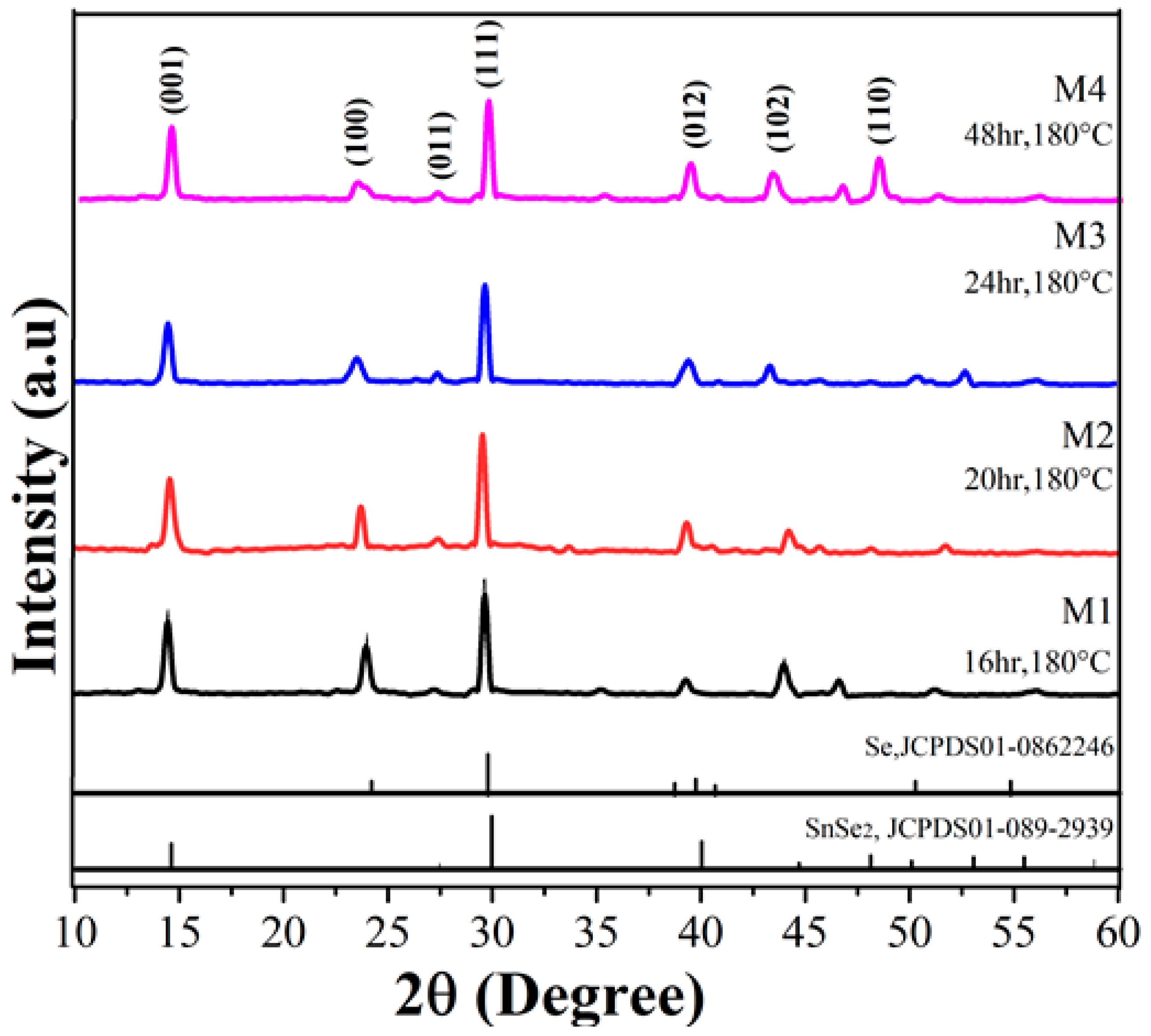
The XRD results for all four samples are shown in Figure 1. It is clear from the XRD data that all of our samples had some fraction of unreacted Se, which is a common problem during the synthesis of various Se containing chalcogenides. The XRD results showed that the major phase of all samples was SnSe2, which further confirmed the successful formation of the SnSe2 structure. It was also noticeable in the XRD spectra that as we increased the reaction time, the presence of Se decreased, which can be seen from the intensity reduction of the Se peak at around 24 degrees 2theata.
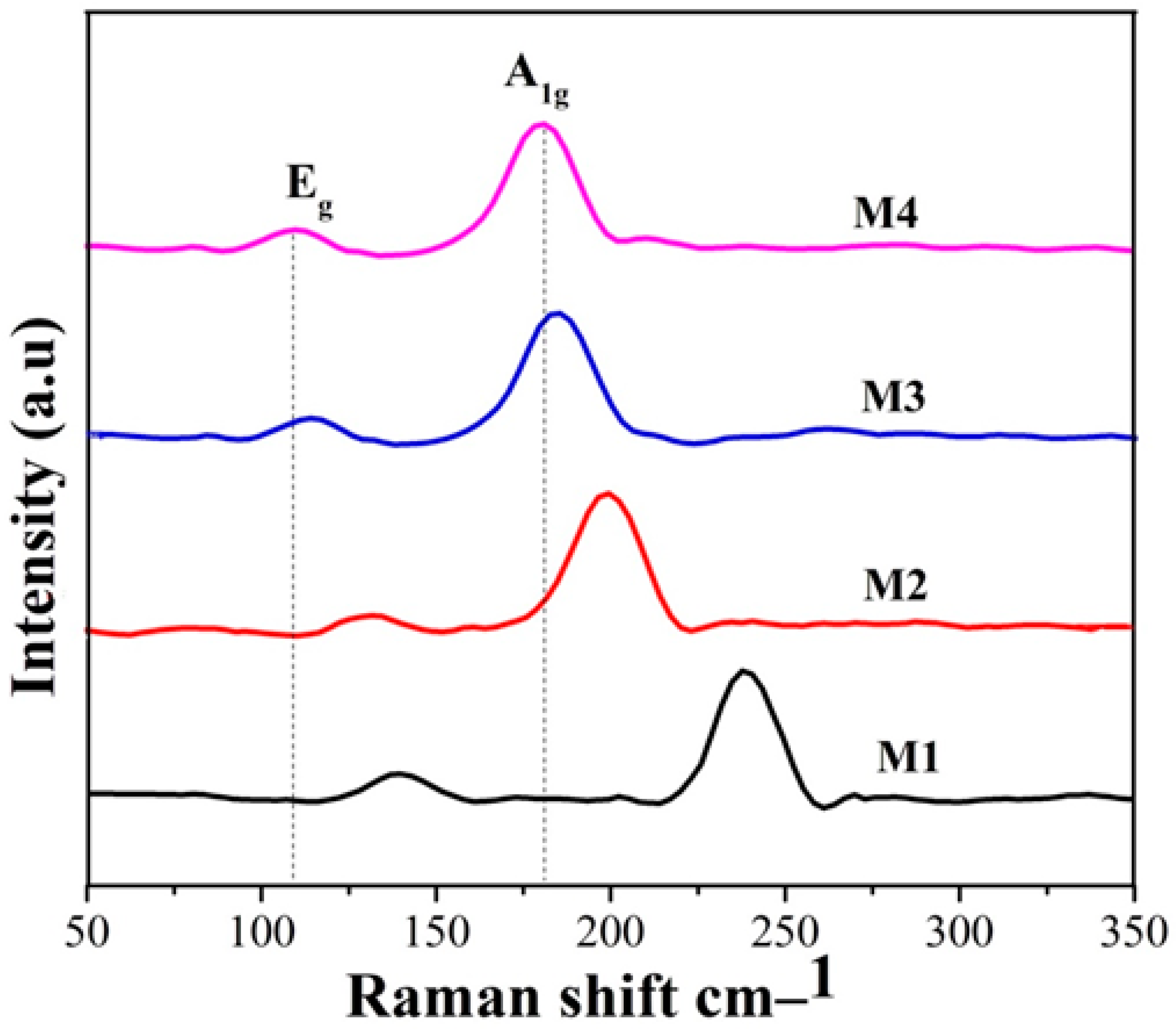
Raman spectroscopy was used to look for any impurity present in the SnSe2 structure and confirm the XRD findings of the SnSe2 nano structured thin films, as shown in Figure 2. The characteristic spectra were recorded at room temperature in the range of Raman shift from 50 to 350 cm−1 while the exciting photon energy was 2.41 ev. These peaks were achieved by using the laser excitation wavelength of 532 nm. The first peak indicates that the Eg mode was almost at 148.6 cm−1, and the second peak corresponding to the A1g mode was the wide peak at around 240 cm−1 for the M1 sample. The actual positions of the pure SnSe2 Raman shifts were around 115 cm−1 and 170 cm−1, respectively, as obtained for sample M4.
The overall spectra shifted toward lower values of the Raman shift as the reaction time was increased and the Raman shifts aligned more with the pure SnSe2 Raman spectra. From these observations, it can be concluded that at low reaction time, some unreacted Se was present in the samples, which had decreased with increasing reaction time. The Raman results support the overall XRD analysis.
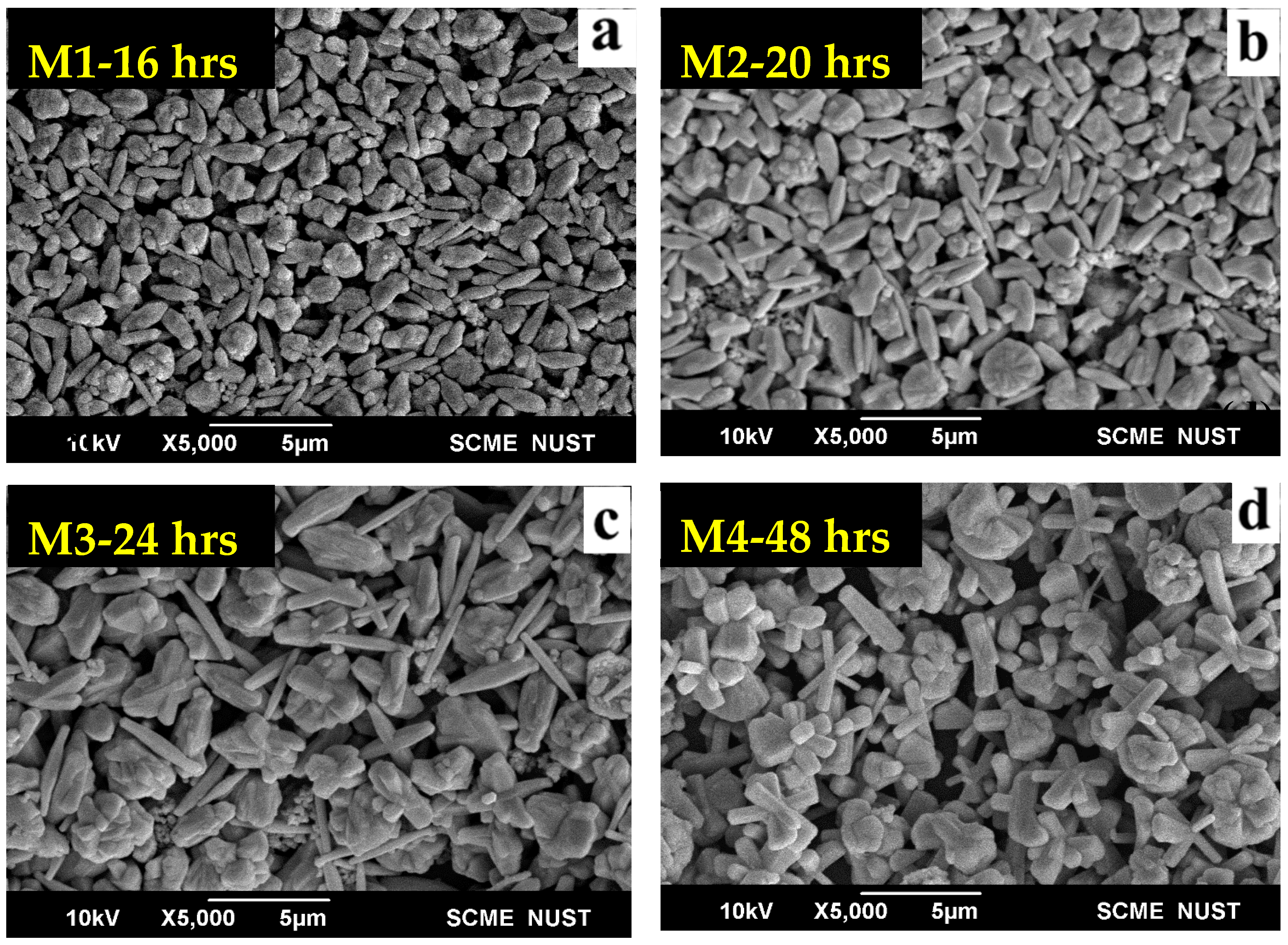
Morphology was an important parameter in this study as we were interested in looking for any morphological effect on the thermal and electronic transport properties of the synthesized SnSe2 structures. Figure 3 shows the SEM images of the SnSe2 thin films annealed at 300 °C for 30 min in the presence of nitrogen. Figure 3a shows that the overall morphology of the sample consisted of irregular agglomerates with few elongated structures. Figure 3b shows that with the increase in reaction time from 16 to 20 h, the agglomerated types of structures started to elongate in the form of a rod type morphology. With further increase in reaction time at 24 h, the mix morphology consisting of flowers and rods could be easily identified from the SEM micrograph in Figure 3c. When the reaction time was increased up to 48 h, the flower type morphology became the dominant form, as shown in Figure 3d. The presence of rods were actually unreacted Se, which grew in the form of the rod type morphology and it was confirmed from the XRD results that with increasing time, the amount of Se was reduced. This argument may well be supported with the help of Raman analysis where the peaks at 240 cm−1 in M1 slightly shifted toward the left side, which indicates the reduction in unreacted Se present in the sample and increase in phase purity of the SnSe2 structure.
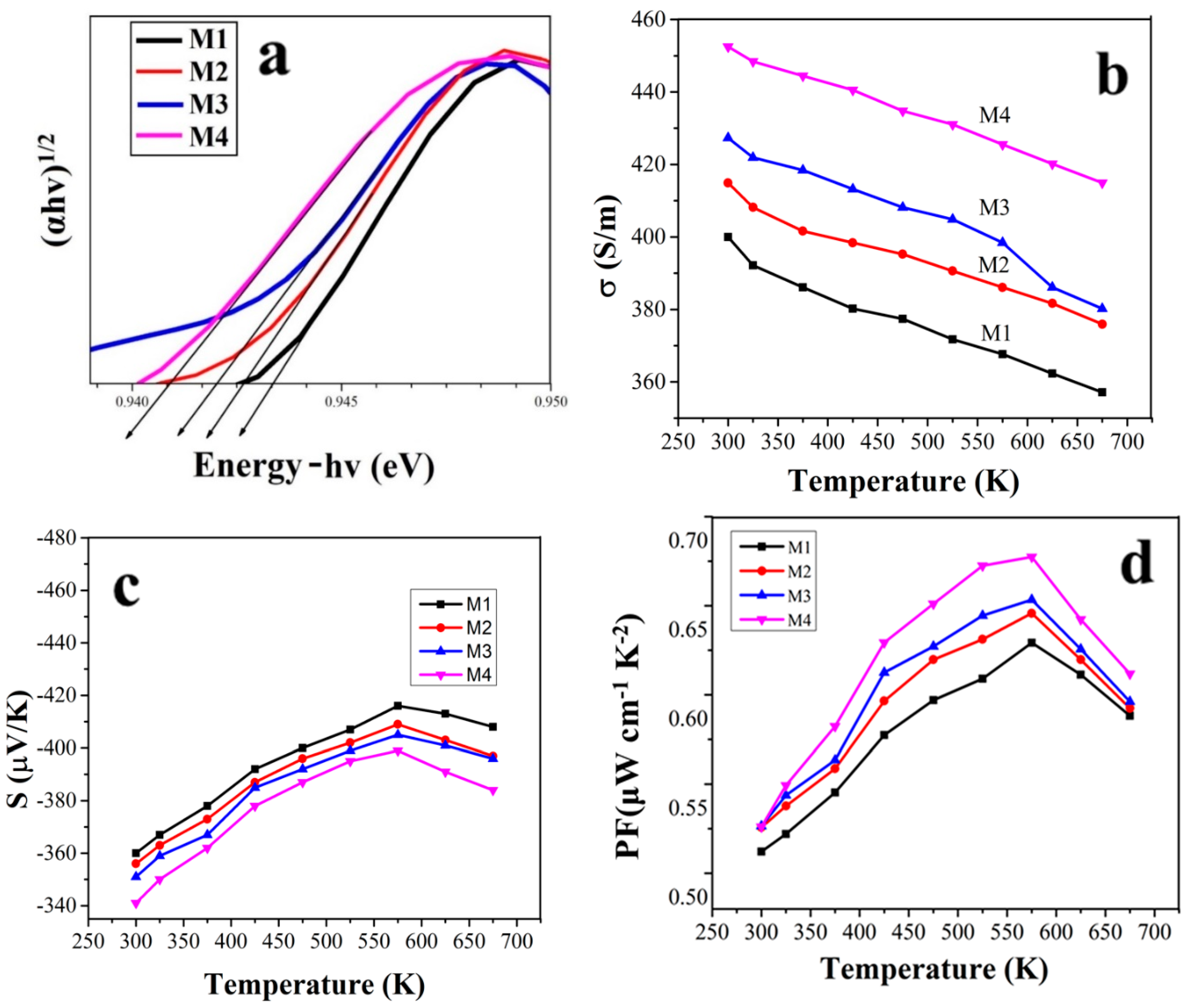
The band gap of the thin film of SnSe2 was obtained from the UV–Vis absorption spectra shown in Figure 4a. The optical absorption coefficient can be calculated from the equation
where t is the thickness of the thin film.
is the absorbance of the sample; Eg is the band gap of the material; is the photon energy; n is the transition coefficient; and A is the absorption constant [18]. The band gap of the material can be extracted by extending the linear region of the graph along the hν axis. The band gap is determined by the intercept along the hν. Figure 4a shows the Tauc plot of different samples vs. () ² for thee SnSe2 thin film samples. The band gap analysis of the SnSe2 samples shows that when we increased the reaction time from 16 to 48 h, the band gap was slightly reduced. Here, it is noticeable that in band gap analysis via Tauc plot, the values may not be highly reliable but relative variation in these band gap values are important and can lead to some understanding regarding the materials’ properties. The trend of electrical conductivity (σ) for the four samples in Figure 4b can be explained well from the band gap analysis of the corresponding samples.
As we see here, the values of σ for sample M1 was lower among them all while the highest values were obtained for sample M4. The thermoelectric properties of the SnSe2 thin films were measured along the substrate surface from 300 to 675 K, as shown in Figure 4b. In all the SnSe2 samples, the σ values showed a semiconducting nature while metallic transport behavior was observed for the Seebeck coefficient (S). In agreement with the band gap analysis, the σ values increased from M1 to M4 at any measured temperature. As usually expected, σ slowly decreased with increasing measuring temperature, in congruence with the increase in Seebeck coefficient for all samples. Thermally activated electrical transport behavior was observed at around 550 K for all the measured SnSe2 samples, where the Seebeck coefficient values started to follow the down trend compared to the readings at lower temperatures. The increment in the Seebeck coefficient at the start is due to the decrease in the Fermi level, and the decline after 550 K is due to the bipolar effect [19,20,21]. We performed Hall resistivity measurements to confirm that the majority of charge carriers were electrons in all samples, which are discussed in later sections. The negative values of the Seebeck coefficient for all the SnSe2 samples further confirmed the n-type semiconductor nature for these samples, as shown in Figure 4c. The peak Seebeck coefficient values were in the range of 380 to 420 µV K−1 at around 550 K, which are favorable values for any good thermoelectric material, but at the same time, our electrical conductivity values were not that high for the same temperature range. Hence, the thermoelectric power (PF) was not that much higher for all of these samples, as shown in Figure 4d. The peak PF along the ab plane was 0.69 μWcm−1K−2 for the M4 sample at 580 K, which was the highest among all of the measured samples. Enhancement in power factor was made possible due to a good increase in σ without largely affecting S. The achievement of controlled S can be attributed to the resulting interface barriers due to a flower like morphology obtained for the samples M3 and M4. These potential barriers improve the filtering process of low energy carriers at the grain boundaries which leads to control of the S values. Thus, the increase in overall power factor of the M4 sample was the result of the synergistic effect of morphology on the σ and S, where we obtained prominent enhancement in σ without largely compromising the S values [22,23,24]. The observed PF values in this work are in the range of the previously reported literature for the SnSe2 structures [25,26]. The overall study suggests that as the reaction time increased, the phase purity was enhanced for the SnSe2 structure and led to higher σ and PF.
4. Conclusions
We successfully synthesized the SnSe2 structure via the solvothermal route and achieved somewhat control over its morphology by varying the reaction time. The solvothermal synthesis route was selected due its good control on the morphology and microstructure. We investigated the thermoelectric properties of the synthesized samples and found that phase purity and morphology can affect its thermoelectric performance. The comparatively larger PF value of sample M4 can be related to the increase in its electrical conductivity due to the increase in phase purity and band gap reduction. The key finding of the study is that as the reaction time was increased, the phase purity was enhanced for the SnSe2 structure and led to a higher σ and PF.
Author Contributions
Idea and experimentation design, M.S. and M.F.; writing and original draft preparation, M.S., M.F. and H.K.; Formal Analysis, M.S., M.F., M.A.U. and W.H.T.; Investigation, M.F. and H.K.; Resources, M.A.U., W.H.T. and A.S.; Review and Editing, M.A.U., W.H.T. and A.S.; Supervision, M.S. All authors have read and agreed to the published version of the manuscript.
Funding
This research received no external funding.
Conflicts of Interest
The authors declare no conflict of interest.
References
- Minnich, A.J.; Dresselhaus, M.S.; Ren, Z.F.; Chen, G. Bulk nanostructured thermoelectric materials: Current research and future prospects. Energy Environ. Sci. 2009, 2, 466. [Google Scholar] [CrossRef]
- Mahan, G.D. Introduction to thermoelectrics. APL Mater. 2016, 4, 104806. [Google Scholar] [CrossRef]
- Shi, X.; Yang, J.; Salvador, J.R.; Chi, M.; Cho, J.Y.; Wang, H.; Bai, S.; Yang, J.; Zhang, W.; Chen, L. Multiple-Filled Skutterudites: High Thermoelectric Figure of Merit through Separately Optimizing Electrical and Thermal Transports. J. Am. Chem. Soc. 2012, 134, 2842. [Google Scholar] [CrossRef]
- Hung, L.T.; Nong, N.V.; Linderoth, S.; Pryds, N. Segmentation of low-cost high efficiency oxide-based thermoelectric materials. Phys. Status Solidi (a) 2015, 212, 767–774. [Google Scholar] [CrossRef]
- Wolf, M.; Hinterding, R.; Feldhoff, A. High Power Factor vs. High zT—A Review of Thermoelectric Materials for High-Temperature Application. Entropy 2019, 21, 1058. [Google Scholar] [CrossRef] [Green Version]
- Shuai, J.; Mao, J.; Song, S.; Zhu, Q.; Sun, J.; Wang, Y.; He, R.; Zhou, J.; Chen, G.; Singh, D.J.; et al. Tuning the carrier scattering mechanism to effectively improve the thermoelectric properties. Energy Environ. Sci. 2017, 10, 799–807. [Google Scholar] [CrossRef]
- Zhao, L.-D.; Dravid, V.P.; Kanatzidis, M.G. The panoscopic approach to high performance thermoelectrics. Energy Environ. Sci. 2014, 7, 251–268. [Google Scholar] [CrossRef]
- Achimovičová, M.; Silva, K.L.D.; Daneu, N.; Rečnik, A.; Indris, S.; Hain, H.; Scheuermann, M.; Hahn, H.; Šepelák, V. Structural and morphological study of mechanochemically synthesized tin diselenide. J. Mater. Chem. 2011, 21, 5873. [Google Scholar] [CrossRef]
- Shinde, P.; Rout, C.S. Advances in synthesis, properties and emerging applications of tin sulfides and its heterostructures. Mater. Chem. Front. 2021, 5, 516–556. [Google Scholar] [CrossRef]
- Cain, J.D.; Hanson, E.D.; Shi, F.; Dravid, V.P. Emerging opportunities in the two-dimensional chalcogenide systems and architecture. Curr. Opin. Solid State Mater. Sci. 2016, 20, 374–387. [Google Scholar] [CrossRef]
- Bletskan, D. Electronic structure of 2H-SnSe2: Ab initio modeling and comparison with experiment. Semicond. Phys. Quantum Electron. Optoelectron. 2016, 19, 98–108. [Google Scholar] [CrossRef] [Green Version]
- Shafique, A.; Samad, A.; Shin, Y.-H. Ultra low lattice thermal conductivity and high carrier mobility of monolayer SnS2 and SnSe2: A first principles study. Phys. Chem. Chem. Phys. 2017, 19, 20677–20683. [Google Scholar] [CrossRef] [PubMed]
- Rahman, A.; Kim, H.J.; Noor-A-Alam, M.; Shin, Y.-H. A theoretical study on tuning band gaps of monolayer and bilayer SnS2 and SnSe2 under external stimuli. Curr. Appl. Phys. 2019, 19, 709–714. [Google Scholar] [CrossRef]
- Huang, Y.; Xu, K.; Wang, Z.; Shifa, T.A.; Wang, Q.; Wang, F.; Jiang, C.; He, J. Designing the shape evolution of SnSe2nanosheets and their optoelectronic properties. Nanoscale 2015, 7, 17375–17380. [Google Scholar] [CrossRef] [PubMed]
- Ding, Y.; Xiao, B.; Tang, G.; Hong, J. Transport Properties and High Thermopower of SnSe2: A Full Ab-Initio Investigation. J. Phys. Chem. C 2016, 121, 225–236. [Google Scholar] [CrossRef]
- Tyagi, K.; Gahtori, B.; Bathula, S.; Singh, N.K.; Bishnoi, S.; Auluck, S.; Srivastava, A.K.; Dhar, A. Electrical transport and mechanical properties of thermoelectric tin selenide. RSC Adv. 2016, 6, 11562–11569. [Google Scholar] [CrossRef]
- Schrade, M.; Fjeld, H.; Norby, T.; Finstad, T.G. Versatile apparatus for thermoelectric characterization of oxides at high temperatures. Rev. Sci. Instrum. 2014, 85, 103906. [Google Scholar] [CrossRef] [PubMed]
- Assili, K.; Gonzalez, O.; Alouani, K.; Vilanova, X. Structural, morphological, optical and sensing properties of SnSe and SnSe2 thin films as a gas sensing material. Arab. J. Chem. 2020, 13, 1229–1246. [Google Scholar] [CrossRef]
- Gibbs, Z.M.; Kim, H.-S.; Wang, H.; Snyder, G.J. Erratum: “Band gap estimation from temperature dependent Seebeck measurement—Deviations from the 2e|S|maxTmax relation” [Appl. Phys. Lett. 106, 022112 (2015)]. Appl. Phys. Lett. 2016, 108, 209901. [Google Scholar] [CrossRef] [Green Version]
- Hong, M.; Wang, Y.; Feng, T.; Sun, Q.; Xu, S.; Matsumura, S.; Pantelides, S.T.; Zou, J.; Chen, Z.-G. Strong Phonon–Phonon Interactions Securing Extraordinary Thermoelectric Ge1–xSbxTe with Zn-Alloying-Induced Band Alignment. J. Am. Chem. Soc. 2018, 141, 1742–1748. [Google Scholar] [CrossRef]
- Hong, M.; Lyv, W.; Li, M.; Xu, S.; Sun, Q.; Zou, J.; Chen, Z.G. Rashba Effect Maximizes Thermoelectric Performance of GeTe Derivatives. Joule 2020, 4, 2030–2043. [Google Scholar] [CrossRef]
- Akshay, V.R.; Suneesh, M.V.; Vasundhara, M. Tailoring Thermoelectric Properties through Structure and Morphology in Chemically Synthesized n-Type Bismuth Telluride Nanostructures. Inorg. Chem. 2017, 56, 6264–6274. [Google Scholar] [CrossRef] [PubMed]
- Hong, M.; Zheng, K.; Lyv, W.; Li, M.; Qu, X.; Sun, Q.; Xu, S.; Zou, J.; Chen, Z.-G. Computer-Aided Design of High-Efficiency Gete-Based Thermoelectric Devices. Energy Environ. Sci. 2020, 13, 1856–1864. [Google Scholar] [CrossRef]
- Hong, M.; Lyu, W.; Wang, Y.; Zou, J.; Chen, Z.G. Establishing the Golden Range of Seebeck Coefficient for Maximizing Thermoelectric Performance. J. Am. Chem. Soc. 2020, 142, 2672–2681. [Google Scholar] [CrossRef] [PubMed]
- Xu, P.; Fu, T.; Xin, J.; Liu, Y.; Ying, P.; Zhao, X.; Pan, H.; Zhu, T. Anisotropic thermoelectric properties of layered compound SnSe2. Sci. Bull. 2017, 62, 1663–1668. [Google Scholar] [CrossRef] [Green Version]
- Pham, A.-T.; Vu, T.H.; Cheng, C.; Trinh, T.L.; Lee, J.-E.; Ryu, H.; Hwang, C.; Mo, S.-K.; Kim, J.; Zhao, L.-D.; et al. High-Quality SnSe2 Single Crystals: Electronic and Thermoelectric Properties. ACS Appl. Energy Mater. 2020, 3, 10787–10792. [Google Scholar] [CrossRef]
Figure 1.
XRD pattern of the SnSe2 nano structured thin films synthesized via the solvothermal route. The four names of the samples represent different morphologies of the SnSe2 structure with different reaction time.
Figure 1.
XRD pattern of the SnSe2 nano structured thin films synthesized via the solvothermal route. The four names of the samples represent different morphologies of the SnSe2 structure with different reaction time.

Figure 2.
Raman spectra of SnSe2 nano structured thin films calculated from 50 to 350 cm−1 synthesized via thee solvothermal route. Eg and A1g represent the different molecular vibrations due to bonds present in the structure.
Figure 2.
Raman spectra of SnSe2 nano structured thin films calculated from 50 to 350 cm−1 synthesized via thee solvothermal route. Eg and A1g represent the different molecular vibrations due to bonds present in the structure.

Figure 3.
SEM micrographs of the SnSe2 thin films drop casted on a glass substrate. The variation in morphologies with increased reaction time can easily be seen. M1 represent the sample with reaction time of 16 h (a), M2, 20 h (b), M3 reaction time was 20 h (c) and M4 reaction time was 48 h as shown in (d).

Figure 4.
(a) Band gap analysis in form of a Tauc plot of the synthesized four samples. Temperature dependent electrical conductivity (b), Seebeck coefficient (c), and power factor (d) of the solvothermally synthesized SnSe2 thin films.
Figure 4.
(a) Band gap analysis in form of a Tauc plot of the synthesized four samples. Temperature dependent electrical conductivity (b), Seebeck coefficient (c), and power factor (d) of the solvothermally synthesized SnSe2 thin films.

Publisher’s Note: MDPI stays neutral with regard to jurisdictional claims in published maps and institutional affiliations. |
© 2021 by the authors. Licensee MDPI, Basel, Switzerland. This article is an open access article distributed under the terms and conditions of the Creative Commons Attribution (CC BY) license (https://creativecommons.org/licenses/by/4.0/).
Share and Cite
MDPI and ACS Style
Siyar, M.; Farid, M.; Khan, H.; Umar, M.A.; Tanveer, W.H.; Safdar, A. Controlled Morphology and Its Effects on the Thermoelectric Properties of SnSe2 Thin Films. Crystals 2021, 11, 942. https://doi.org/10.3390/cryst11080942
AMA Style
Siyar M, Farid M, Khan H, Umar MA, Tanveer WH, Safdar A. Controlled Morphology and Its Effects on the Thermoelectric Properties of SnSe2 Thin Films. Crystals. 2021; 11(8):942. https://doi.org/10.3390/cryst11080942
Chicago/Turabian StyleSiyar, Muhammad, Maroosha Farid, Haad Khan, Malik Adeel Umar, Waqas Hassan Tanveer, and Amna Safdar. 2021. "Controlled Morphology and Its Effects on the Thermoelectric Properties of SnSe2 Thin Films" Crystals 11, no. 8: 942. https://doi.org/10.3390/cryst11080942
Note that from the first issue of 2016, this journal uses article numbers instead of page numbers. See further details here.