Triple-Mesoscopic Carbon Perovskite Solar Cells: Materials, Processing and Applications


SPECIFIC, Swansea University, Bay Campus, Swansea SA1 8EN, UK
*
Author to whom correspondence should be addressed.
Energies 2021, 14(2), 386; https://doi.org/10.3390/en14020386
Submission received: 17 December 2020
/
Revised: 6 January 2021
/
Accepted: 7 January 2021
/
Published: 12 January 2021
(This article belongs to the Section A2: Solar Energy and Photovoltaic Systems)
Abstract
:Perovskite solar cells (PSCs) have already achieved comparable performance to industrially established silicon technologies. However, high performance and stability must be also be achieved at large area and low cost to be truly commercially viable. The fully printable triple-mesoscopic carbon perovskite solar cell (mCPSC) has demonstrated unprecedented stability and can be produced at low capital cost with inexpensive materials. These devices are inherently scalable, and large-area modules have already been fabricated using low-cost screen printing. As a uniquely stable, scalable and low-cost architecture, mCPSC research has advanced significantly in recent years. This review provides a detailed overview of advancements in the materials and processing of each individual stack layer as well as in-depth coverage of work on perovskite formulations, with the view of highlighting potential areas for future research. Long term stability studies will also be discussed, to emphasise the impressive achievements of mCPSCs for both indoor and outdoor applications.
1. Introduction
Perovskite solar cells (PSCs) represent an exciting new thin-film technology [1,2,3,4,5,6]. There are potentially a vast number of creative applications for perovskites, and these devices are perhaps uniquely versatile in that PSCs have achieved high efficiencies in a variety of different architectures [7,8,9,10]. PSC architectures have use of mesoporous layers and planar structures, and swapped or completely eliminated the charge transport layers [11]. This is possible because of the intrinsic perovskite ambipolarity [12,13].
The triple-mesoscopic carbon PSC (mCPSC) is unusual compared to other thin-film PSC architectures. First introduced in 2013 by Han and co-workers [14], devices consist of a triple-mesoscopic stack consisting of a mesoporous electron transport layer (ETL) (TiO2), mesoporous insulating layer (usually ZrO2) and a porous, conductive carbon top contact. No hole transport layer (HTL) is required in this architecture. Layers are screen-printed onto a conductive glass substrate coated with compact TiO2 and annealed at high temperature to remove organic binders before subsequent infiltration of the perovskite ink. This means that the perovskite is hosted in all the three layers of the micrometre-thick stack, as opposed to being a sandwich structure between very thin electrodes (Figure 1).
Under light, photogenerated electrons are injected into the TiO2, which is in close contact with the transparent electrode. Holes are transferred through the perovskite in the insulating layer and must travel several micrometers before injection into the carbon (Figure 2). This architecture, therefore, reveals that photogenerated electron-hole pairs in perovskites have remarkably long lifetimes.
As the entire stack is fully printable, mCPSCs have high potential for scale-up. The rigid glass substrates, used as they can withstand high temperature annealing, are most suited to sheet-to-sheet (S2S) batch production. The screen-printing processes commonly used to print the stack are also particularly well suited to S2S manufacture, although a roll-to-roll (R2R) production is feasible via rotary screen-printing. Layers can be also deposited via slot-die coating [17], which would be ideal for a R2R process on flexible substrates. The manufacture of mCPSC on flexible substrates is still limited by the high curing temperature (>400 °C), but it represents a fascinating challenge for future research.
The thermal treatment can be optimised via near-infrared (NIR) fast annealing for rapid production and low energy consumption. This fast annealing can decrease the cost of production [15]. Module interconnects can be accurately created via a low-cost rapid material removal approach known as the scribing method. With the use of screen-printing, scribing method and fast annealing process such as Near-Infrared (NIR) a possible production line emerges, schematically shown in Figure 3.
Other PSCs with non-porous carbon top electrodes atop the perovskite layer in conventional sandwich structure have also been proposed [18]. In these devices, the carbon directly replaces the metal top contact of a typical PSC, allowing the preparation of low temperature devices. This is a potential advantage over mCPSCs, which require high temperature annealing to remove organic paste binders and form the porous stack [19]. Consequently, mCPSCs have yet to be deposited on flexible substrates such as PET, while this has been already achieved with the other carbon architectures [20].
However, these devices often exhibit inferior stability (Section 4). Furthermore, chemical interactions between the perovskite crystals and some carbon inks can cause degradation or poor performance [15,21]. This is not a problem in mCPSCs, as binder is burned away before perovskite infiltration, allowing for more flexibility when designing ink formulations.
Another advantage of the mCPSC is the potential for pre-fabricating a large number of stacks on glass and infiltrating the perovskite precursor solution as needed to produce devices on demand. This characteristic allows for the preparation of preassembled products and would enable fast delivery in an industrial setting. Finally, the mCPSC is low-capital cost as all the required equipment to deposit the layers on a glass/FTO/compact TiO2 substrate is inexpensive (FTO, F:SnO2). The low-capital cost is a key aspect of this technology—although expensive equipment, such as high-tech screen-printers or NIR heating elements can be used for high volume production, extremely low-cost equipment can also be applied, especially when mechanical scribes or manual screen printers are adopted. In other words, the lab-to-fabrication process is cheaper and easier than for other PSC architectures, and the small initial investment has the potential to pay back over a shorter period for both large companies and small enterprises.
Interest in mCPSCs has therefore increased rapidly due to the high potential for achieving short-term market penetration [22,23]. In particular:
- Screen-printing is an established industrial method for large volume production and up-scaling mCPSC manufacture is therefore straightforward. As mentioned above, equipment is also inexpensive, decreasing the financial risks associated with production line setup.
- Low material costs—unlike in many conventional PSCs, expensive noble metals and organics that require costly purification processes (like spiro-OMeTAD) are not required [24];
- Module performance is not particularly affected by the size of the device, as often happens for other PSC architecture [29].
Modules, i.e., devices based on single cells linked by an interconnect, can be prepared via a pure registration approach [30,31] or scribing [32,33]. Crucial in large area devices, interconnects help overcome the issue of the resistance introduced by large substrates. Interconnects can be used to create parallel or series-connected modules to allow charge collection close as possible to the generation point.
The registration method exploits the ability of printing technologies to pattern each layer. When these layers are accurately registered in the exact designed position, it is possible to create interconnects during the initial print. Printing must be incredibly accurate, as any misalignment can cause shorts between layers. Print precision relies on the technology of the screen-printer. The accuracy of a given printer may be enhanced using camera systems and software, however this can increase cost and/or slow down the production rate.
Alternatively, in the scribing method layers are deposited as solid areas and then scribed using a blade or a laser, to disconnect specific layers or open an aperture for interconnects. Three scribes called P1, on the bottom electrode, P2, through the mesoporous TiO2 and ZrO2 layers, and P3, on the top electrode, create the necessary interconnection in a series-connected module (Figure 4). A material removal approach that requires less expensive equipment, the scribing method can be much faster than the registration method and suits either a S2S or a R2R production. This method is widely used in thin film solar modules with high active/substrate area ratio (geometric fill factor, g-FF).
Perhaps the least inherently scalable step in mCPSC manufacture is the infiltration of the perovskite ink. This is usually done via drop casting at lab scale. The method is quick and simple when making small single cells, but it is prone to human error and becomes time-consuming and complex at larger scale. Alternative methods suitable for larger devices and high throughput production have been explored, including inkjet printing [34,35], robotic dispensers and mesh (RbM) [31,32,36] and slot-die coating [33,37].
The mCPSCs have also many interesting avenues for fundamental research. For example, exceptional stability has been observed with the addition of 5-aminovaleric acid (NH3(CH2)4COOH+, AVA) into methylammonium lead iodide perovskite (CH3NH3PbI3, MAPbI3) [25,28]. This resulted in astonishing stability results, with devices passing IEC61215:2016 standards and 9000 h under maximal power point tracking without degradation [28]. The importance of the perovskite formulation and the work done in recent years in advancing performance and stability will be discussed in detail in Section 3. Many aspects related to the high stability of mCPSCs, such as the long charge lifetime and the surprising benefits of high humidity device exposure [38] require clarification.
2. Modifications to the Triple Mesoscopic Stack
The chemical, physical and morphological properties of the inorganic mesoporous stack play an important role in determining device performance. The most influential variations in the inorganic stack trialled thus far are reported in this section.
2.1. TiO2 Layer
TiO2 is present in the mCPSC architecture as both a compact and mesoporous layer, and respectively act as a hole barrier and electron transporting layer (ETL). Despite much research on alternative ETLs for other devices [39,40,41], TiO2 is so far the only n-type material tested in mCPSCs, leaving this area open to further investigation. Both band alignment and thermal stability are important characteristics mCPSC ETLs, as layers are subject to multiple high temperature annealing steps to remove binders and create the porous scaffold.
Compact layer thickness heavily impacts performance, with a particularly large effect on device hysteresis [42]. However, the effect of changing ETL morphology, chemical composition or doping has yet to be explored in depth.
The mesoporous layer tends to be between 0.4 µm and 1 µm thick [27,30,43,44], and provides a very large interface with the perovskite to maximise charge extraction [27,30,43,45]. In 2017 Priyadarshi et al. reported a simplified architecture without this layer, showing working devices with reduced power conversion efficiencies (PCE). The observed performance reduction can be minimised by using thicker ZrO2 to compensate for the loss of the mesoporous TiO2 layer [46]. Specifically, when ZrO2 was increased from 1.4 to 2.1 µm, devices achieved nearly the same performance as controls incorporating a standard 0.5 µm TiO2 layer (11.9% PCE standard architecture, 7.8% PCE without TiO2, and 9.7% PCE with thicker ZrO2).
In terms of nanoparticle size, an optimal dimension of 20–30 nm in diameter allows large pore sizes for effective infiltration [16]. Mixed size nanoparticle systems (25 nm and 100 nm) have been shown to further increase layer porosity and improve perovskite infiltration [47]. It is also possible to enhance device performance through incorporating additional materials into the mesoporous TiO2. For example, Xu and co-workers added EuW10, a luminescence down-conversion material, to the TiO2 paste before printing [48], resulting in a PCE improvement from 11.42% to 14.36% due to increases in short circuit current (Jsc) and fill factor (FF).
Very recently, Sheng et al. presented a simple and effective method to modify the ETL and improve the device photovoltage. Annealed stacks were treated with 2-phenyl-5-benzimidazole sulfonate-Na before infiltration, to shift the TiO2 conduction band from −4.22 to −4.11 eV. As a result, the electron transfer from the perovskite absorber to the ETL was enhanced and recombination at the ETL/perovskite interface suppressed. Consequently, the open circuit voltage (Voc) and FF of the devices were increased without sacrificing the Jsc, with the champion device showing an overall PCE of 16.51% [49].
2.2. Insulating Layer
The insulating or spacer layer is crucial to the mCPSC as it separates the ETL from the top electrode. This prevents the formation of a TiO2/carbon interface, which would act as a Schottky diode and drive recombination. This layer is not present in other architectures, where either an HTL, ETL or perovskite capping layer provides the necessary separation [13,18,50,51]. In principle, the spacer layer can consist of any insulating material thermally stable enough to survive the high temperature treatments used to remove paste binders. The most widely adopted material is ZrO2, although Al2O3 and SiO2 have also been reported.
Layer thickness is important—the spacer should be thick enough to avoid any pinholes and properly separate the carbon from the TiO2, while being thin enough not to hinder charge transport or infiltration. According to early reports, the optimal spacer thickness for TiO2/ZrO2/carbon stacks infiltrated with MAPbI3 is between 1 and 1.4 µm [52]. Another optimisation study on AVA-MAPbI3 devices by Hu et al. on a 0–4 µm ZrO2 range with perovskite found that a 2 µm ZrO2 layer exhibited optimal performance [30].
However, efficient AVA-MAPbI3 devices of over 15% PCE can be achieved with 3 µm spacer layer, as reported by Han and co-workers [53,54]. It appears that as long as the stack is well-infiltrated, devices with 2 or 3 µm thick ZrO2 layers show better performance than those with a 1.2 µm [54]. Optimal ZrO2 thickness for TiO2/ZrO2/carbon-AVA-MAPbI3 mCPSC was systematically investigated by Liu et al. [55]. With an optimised ZrO2 nanoparticle size of 20 nm, nearly 14% PCE was achieved with a 4.84 µm spacer layer. In other words, although high quality infiltration becomes more challenging as the thickness of the spacer layer increases, when good infiltration is achieved, better performance is observed with a thicker insulating layer (Figure 5).
The effect of increasing spacer layer thickness is incredibly unexpected and reveals several interesting perovskite properties. As most photogenerated charge is generated in the first few hundred nanometres of the stack [56], holes must travel extreme distances through the perovskite before collection at the carbon electrode. The path through the insulator layer is even longer than the layer is thick, as charges are limited to travelling between perovskite crystals in the mesoporous framework. Holes must therefore travel several µm simply to cross the insulating layer. As these distances are far larger than typical perovskite diffusion lengths it would be logical to assume that devices would exhibit low PCEs due to high levels of recombination. However, this is not the case: despite the long distance, enough charge can be extracted and collected to achieve over 13% PCE, and the best results are often observed with thicker spacers. The reason for such performance enhancements is still unclear.
The effect of spacer layer thickness on PCE has been most thoroughly investigated for the TiO2/ZrO2/carbon-AVA-MAPbI3 devices discussed above. However, it should be noted that optimal spacer thickness can vary when alternative perovskite formulations are used. For example, Cs0.1Rb0.05FA0.85PbI3 perovskite formulations achieved an outstanding 16% PCE with a ZrO2 layer of only 750 nm [57]. Alternatively, a 17% PCE device using Cs0.05(FA0.4MA0.6)0.95PbI2.8Br0.2 perovskite was reported in 2017 with optimised layer thicknesses of 460 nm, 450 nm, 800 nm and 10 µm for TiO2/Al2O3/NiO and carbon layers respectively [58]. Conversely, a study by Di Carlo and co-workers in 2019 found that a 1.2 µm thick Al2O3 was optimum for MAPbI3 devices [59], with optimised devices of around 9.13% PCE compared to 8.28% for 0.8 µm and 6.29% for 1.8 µm.
Thinner, sputtered Al2O3 spacer layers in the order of hundreds of nm for AVA-MAPbI3 devices have also recently been reported, proving that that mCPSCs can work without very thick spacer layers as long as the carbon layer is properly insulated [60]. Here, Al2O3 at thicknesses of 10, 20, 40 or 100 nm was sputtered onto screen-printed mesoporous TiO2 (Figure 6). Optimal results were observed at 40 nm, with cells exhibiting very high Voc (around 1 V) and comparable overall performance to standard screen-printed ZrO2 devices. Devices with still-thin 100 nm spacer layer performed poorly, probably because a sputtered layer can impede infiltration.
Insulating materials can also be combined. For example, in 2018 Han and co-workers tested 0–20 nm Al2O3 layers in combination with mesoporous screen-printed ZrO2 to improve AVA-MAPbI3 mCPSCs [61]. The Al2O3 was deposited via evaporation of Al onto the mesoporous TiO2 layer and subsequent ambient annealing at 500 °C. Using both 10 nm Al2O3 and screen-printed ZrO2 layers, performance improved to 14% (from 12% without Al2O3) due to increased Voc.
Alternatively, Al2O3 layers of <2.4 nm can be deposited onto the mesoporous TiO2 via spray pyrolysis of aluminium isopropoxide before ZrO2 screen printing [54]. In this work ZrO2 layer thickness was optimised at 3 µm without Al2O3. However, 1.2 µm exhibited similar performance when used in conjunction with Al2O3. As observed in [61], the Al2O3 layer improved Voc, with devices exhibiting around 840 mV for a 1.2 µm ZrO2 layer, 890 mV with the Al2O3 interlayer and 1.2 µm ZrO2 and 920 mV with 3 µm ZrO2 [54].
Al2O3 can be also deposited as a mesoporous layer in substitution to ZrO2, reported to produce an 8% PCE TiO2/Al2O3/carbon-MAPbI3 mCPSC by Xu et al. in 2014 [62]. PCE in these devices was then enhanced by adding p-type dopants or additional layers. For example, the introduction of an NiO interlayer between Al2O3 and carbon resulted in significant PCE improvement in MAPbI3 devices (15.03% PCE from 11.2% without NiO) [63], FA0.4MA0.6PbI2.8Br0.2 devices (14.88% PCE) and Cs0.05(FA0.4MA0.6)0.95PbI2.8Br0.2 devices (17.02% PCE) [58]. Al2O3 has also been used in combination with CNTs in a NiO matrix top electrode [64].
The best choice of oxide for the spacer layer may depend on the chosen perovskite formulation. The AVA-MAPbI3 perovskite for example, is rarely used in combination with Al2O3, and comparative a study for AVA-MAPbI3 devices has shown that ZrO2 significantly outperforms Al2O3 (8.72% over 5.48% PCE) [65]. Some evidence suggests that complex phase dynamics at the TiO2/ZrO2 interface can contribute significantly to AVA-MAPbI3 device performance, which may explain this tendency [66]. Further research is therefore required on whether AVA-MAPbI3 can produce efficient devices in an Al2O3 stack.
An alternative spacer layer to the more conventional ZrO2 and Al2O3 is SiO2. This has proven to be a functional scaffold when mixed with TiO2 in carbon-based sandwich PSCs [67]. In AVA-MAPbI3 mCPSCs, SiO2 spacer layers have been used to produce a 13.1% PCE device [68].
The spacer layer is the main novelty of the mCPSC architecture and introduces many interesting properties, from phase formation to the analysis of long-range charge transport. Its specific role in charge generation and transport currently remains unclear, and the specific interactions between this layer during infiltration and device operation present interesting areas for further research.
2.3. Carbon Top Electrode
Consisting principally of graphite (G) and carbon black (CB), the thickness of the carbon top contact and ratio of constituent carbon materials affects both perovskite precursor infiltration and electrode conductivity. To minimise series resistance, the conductivity of the top layer must be as high as possible without negatively affecting infiltration. This often requires compromise, as properties which improve conductivity often impede infiltration.
For example, carbon electrode conductivity increases with thickness, which is beneficial to device fill factor (FF). Conversely, excessively thick carbon layers can hinder infiltration and negatively affect performance. The same is true for the CB:G ratio, which can also be used to tune layer conductivity and porosity. While CB can increase the layer porosity, it is less conductive than graphite. An optimum CB content in a G:CB formulation is around 20% weight [69]. The size of particle also impacts performance: it has also been found that larger G flakes increase both conductivity and porosity. The optimal size for G flakes was found to be ~9 µm in an 8 µm thick layer [70].
Alternatively, this challenge can be addressed through application of an additional conductive layer to the infiltrated device. As these materials are applied directly onto the annealed perovskite, they must be carefully chosen and annealed at low temperatures so as not to damage the underlying absorber. Initial attempts saw PCE improvements from 12.6% to 14% with the addition of G flakes [71]. An alternative approach is to apply a metallic grid using a second, non-porous carbon ink that does not affect the perovskite performance [72]. The use of Al and Cu metallic grids in this way improved device performance by over 2%—from around ~11% to around ~13%. Device stability was also enhanced, as the additional carbon ink limited environmental exposure of the underlying perovskite. Organic HTL have also been trialled: infiltration of the organic spiro-OMeTAD through the carbon layer of a pre-fabricated mCPSC resulted in efficiency improvements from 9% to 10%, although this significantly increased device cost [73].
Performance may also be enhanced by improving top contact selectivity: the carbon is a poor electron barrier, which can limit hole extraction. This can be improved by raising the layer work-function, usually achieved through chemical modification of the carbon. For example, functionalising with C–OH and C=O groups during carbonisation of the raw materials can raise the carbon work function from 5.0 eV to 5.2 eV [74]. The increase was considered the main contributor to observed device improvements, from 13.6% to 15.7% PCE. Similarly, boron functionalised graphite was found to raise the carbon layer work function from 4.81 eV to 5.10 eV, resulting in a performance increase from around 12.5% to 13.5% [75].
Carbon nanotubes (CNTs) have also been used to improve the hole selectivity. Incorporating hole conducting single walled CNTs (SWCNTs) has produced a MAPbI3 device of In 2016 Wang 14.7% PCE [76]. Alternatively SWCNT can be applied as part of an NiO matrix in the top electrode [64]. A p-type material that can improve hole extraction NiO matrices resulted in PCE enhancement from 10.5% to 12.7%. Notably, the NiO devices achieved this performance with a relatively thin electrode of 1.8 µm, compared to 10 µm for control devices. This material could therefore be used to fabricate high performance devices with alternative perovskite formulations, which can struggle to infiltrate standard thick layers.
Many p type inorganic materials could be used to improve hole extraction in this way. Some examples are WO3, CuS, MoO3, Co2O3 and CuO, proposed in 2018 as potential performance enhancing additives for mCPSC carbon layers [53,77,78]. Inorganic HTLs can also be incorporated as a discrete layer between the insulating layer and carbon electrode as discussed in Section 2.2. The large body of work in improving carbon band alignment proves that compositional manipulation of this layer is a valid and effective route to performance enhancement.
2.4. Additional p-Type Materials
The mCPSC can operate efficiently without a selective HTL, which is advantageous as many PSC HTLs are fabricated with expensive and unstable organic materials such as spiro-OMeTAD. However, the poor selectivity and extreme thickness of the stack also means that device efficiencies still lag behind other PSC architectures. In mCPSCs, photo-generated holes must travel a relatively long distance through the perovskite in the insulating layer before reaching the carbon, increasing the risk of recombination.
A recent optical modelling study found that long wavelength light deeply penetrates the stack before absorption [56]. Light absorption in the depth of the device may generate electron-hole pairs close to the carbon layer, which would be at high risk of surface recombination due to the non-selectivity of the carbon. Incorporating hole-selective materials could therefore significantly improve performance by reducing recombination.
Inorganic NiO appears to be the most promising HTL for mCPSCs: this intrinsic p-type semiconductor has high optical transmittance, a deep-lying valence band (~5.4 eV) and good thermal stability. This material has been incorporated into mCPSCs in several ways. Liu et al. presented a fully printable mCPSC with crystalline NiO nanosheets as a HTL between the ZrO2 and carbon layers [79]. The NiO nanosheets provided superior charge collection and prolonged charge lifetime, resulting in a PCE of 14.2%. Xu et al. also inserted a 480 nm NiO p-type interlayer between the insulating layer and the carbon electrode [80]. The NiO interlayer enhanced the device performance to 14.9% PCE by improving hole extraction, raising device Voc and FF.
NiO interlayers have also been investigated with Al2O3 spacers [63]. The fully printable TiO2/Al2O3/NiO/carbon-MAPbI3 device achieved 15.03% PCE, much higher than the 11.2% standard device (Figure 7). High IPCE and improved FF indicated that the NiO layer (800 nm in this case) improved both charge transport and collection. The performance was further improved when the device was infiltrated with a triple cation perovskite of Cs0.05(FA0.4MA0.6)0.95PbI2.8Br0.2; incorporating Cs+ increased the bandgap and the exciton binding energy, which is beneficial to hole extraction [58]. The Cs0.05(FA0.4MA0.6)0.95PbI2.8Br0.2 based NiO device achieved a PCE of 17.02%, which represents one of the highest recorded efficiencies so far for mCPSCs.
Ultraviolet (UV/O3) treatments can be enhance the properties of NiO HTLs by oxidising Ni2+ to Ni3+ on the layer surface, affecting the electronic distribution of the semiconductor. Fabricated mCPSCs had improved charge extraction attaining a PCE of 12.1% with a 450 nm thick Al2O3 insulating layer [81].
Despite the advantages of this material, NiO-based mCPSCs are still not performance optimised due to the high series resistance (Rs) of NiO films, a consequence of low intrinsic conductivity. This can be improved through partial doping with metals such as copper (Cu), which mitigates associated FF and Jsc losses through increasing the p-type conductivity of the layer. In mCPSCs, Cu:NiOx nanoparticles can improve Jsc and FF values through increasing hole extraction efficiency [37]. Single cells and 100 cm2 modules (active area 70 cm2) with an 80 nm mesoporous Cu:NiOx layer have been fabricated, with champion PCEs of 12.1% compared to 9.75% for HTL free samples. The single cells were only slightly better than the modules: 12.8% with Cu:NiOx, 10.49 with NiO and 9.21% without HTL. This proves that mCPSC up-scaling can be achieved without significant performance loss.
An inorganic hole transporting interlayer of spinel Co3O4 has also been investigated as a recombination supressing HTL for mCPSCs [82]. Devices with 70 nm screen printed Co3O4 interlayers exhibited PCEs of 13.27%, an 18% efficiency enhancement on standard devices. This is attributed to the lower hole charge transfer resistance and reduced recombination at the interface, as proven by photoluminescence (PL) and time resolved PL (TRPL) spectroscopy.
Inorganic HTLs can be also introduced into the carbon ink before printing. Due to its appropriately positioned conduction band (5.2 eV), WO3 nanoparticles have been incorporated into the carbon electrode to promote hole-extraction at the perovskite/carbon interface [78]. Results of electrochemical impedance spectroscopy (EIS), PL and TRPL spectra revealed that the carbon electrode with WO3 exhibited a more efficient charge transport and interfacial transfer than WO3-free devices. This led to a cell with 10.77% PCE, a 40% increase over reference devices. Other materials have been successful in improving the performance in other architectures: for example, 1% CuS doping of carbon pastes for conventional sandwich carbon-based devices (i.e., not mCPSC) increased the average PCE from 8.41% to 10.22% [77]. Scope clearly exists for applying these methods to mCPSCs.
A noteworthy example of an alternative method for introducing HTLs incorporated CuSCN into the perovskite precursor before infiltration [83]. This can be challenging, as adding an HTL into the perovskite solution can negatively impact on its rheological properties, which may cause infiltration issues and incomplete pore filling. In this example, a fully printed TiO2/ZrO2/carbon device infiltrated with a AVA-MAPbI3 with 4 mol% CuSCN showed faster charge extraction, reduced hysteresis and a small improvement in average PCE (from 14% to 14.3%).
A summary of the reported results, materials and techniques reported for devices using MAPbI3 or AVA-MAPbI3 perovskites is offered in Table 1.
3. Modifications to the Perovskite Formulation
3.1. Perovskite Requirements and Infiltration Techniques
As a relatively new and structurally unique architecture, the perovskite requirements of mCPSCs are perhaps less well-understood than those of conventional PSCs. These devices are orders of magnitude thicker than conventional structures and the perovskite is entirely contained within a mesoporous scaffold, meaning no perovskite capping layer is present. This significantly changes the required perovskite properties. In non-mCPSC device structures many additives and deposition techniques for the performance and stability enhancement of conventional sandwich PSCs focus on increasing the grain size, coverage and crystallinity of this capping layer [84,85,86,87].
In mCPSCs, grain size is restricted to that of the scaffold pores. Fast crystallisation to form large grains improves the performance and stability of sandwich PSCs by maximising absorption and decreasing the number of unstable grain boundaries. However, such crystallisation behaviour can be detrimental to mCPSC performance, as crystals can preferentially form above the scaffold or impede infiltration by producing blockages [47,65,88]. Instead, infiltration (the extent to which precursor permeates the stack) becomes a major concern. As the inorganic stack is relatively thick, in the order of micrometres, and the carbon layer is made of large graphite flakes, the infiltration is non-trivial [88]. Devices with poor infiltration are less stable, and exhibit low Jsc and Voc values due to poor interfacial contact and reduced charge collection [88]. The full device stack is usually in excess of 15 µm, and a high performing device requires complete permeation of all three layers with minimal voids. To achieve this, crystallisation must be relatively slow and carefully controlled, rendering common methods such as antisolvent assisted spin coating unsuitable.
To ensure complete infiltration, mCPSC annealing temperatures tend to be far lower than in conventional PSCs, generally ranging from 50 °C–100 °C depending on the perovskite composition [25,89,90]. Coupled with the grain-size restrictions introduced by the scaffold, such long, low temperature processes can lead to unfavourable phase formation; for example, FAPbI3 tends to form the yellow δ-phase in this temperature range [91]. These problems may be addressed by changing processing methods and precursor formulations, as discussed in Section 3.4 [90,92,93,94].
Perovskite morphology and crystallisation dynamics may be influenced during and after annealing through changing process parameters and applying post-crystallisation treatments. Most mCPSC infiltration is performed via drop-casting of perovskite precursors. This can be done using one or two-step methods. A one-step method involves application of a stoichiometric ABX3 solution in γ-butyrolactone (GBL) or in a solution of N,N-dimethylformamide and dimethyl sulfoxide (DMF/DMSO), which directly forms the desired perovskite on solvent removal. In a two-step method, the lead halide (usually in DMF) is infiltrated into the stack and annealed before subsequent reaction with the solvated organic cation in a 2-propanol (IPA) chemical bath (Figure 8).
One-step methods are easier to scale up and involve fewer reagents, advantageous especially when using harmful solvent systems. However, reproducible, high quality infiltration is often more difficult to obtain than with a two-step technique [88] (Figure 8). This can be overcome by using vapour assisted annealing techniques, or additive and solvent engineering, as discussed in the following Section [25,57,90].
Two broad approaches may be taken for chemical modification of the perovskite itself: substitution of component perovskite ions or the introduction of additives. Whereas substitution refers to an ion that sits within the bulk ABX3 lattice framework, additives are either removed during annealing or sit at interfaces or in interstitial sites. The terms are often used interchangeably, possibly because some species can act in both ways, with some of the added material incorporating into the lattice and the rest collecting at grain boundaries and other interfaces [95]. Other molecules, such as AVA, partially integrate into the lattice at grain boundaries via functional groups [27]. These species, as well as those able to act as both additives and substituents will be included in the ‘additives’ section of this review.
A variety of additives and substituents have been successfully incorporated into mCPSC in recent years using one and two-step methods. The following section will highlight these developments to give a detailed overview of advancements in the field.
3.2. Organic Additives
By far the most conspicuous additive is 5-aminovaleric acid (AVA). This molecule can be added in both molar ratio and excess and has been found to improve performance in many distinct ways.
First presented as a perovskite precursor component in 2014 to improve infiltration, cross-sectional analysis has since shown that 3% AVA in a MAPbI3-GBL precursor can improve infiltration by 94% when applied in a one-step deposition (Figure 9). This is achieved by a templating effect, where AVA adsorbs to the metal oxide surface via carboxyl groups, improving precursor wetting and introducing nucleation points. As shown by large increases in IPCE spectra, the small, densely packed crystals observed using transmission electron microscopy (TEM) enhance light absorption and charge extraction at the perovskite-titania interface, resulting in high Jsc and corresponding PCE improvement [25,88].
Better scaffold infiltration can enhance stability through restricting the movement of species such as gaseous methylammonium iodide (MAI) in and out of devices, with MAPbI3 mCPSCs exhibiting longer lifetimes under ambient conditions than classic mesoscopic devices [14]. Similarly, well infiltrated MAPbI3 mCPSCs produced by two-step infiltrations are more resilient to degradation than poorly infiltrated cells [88]. However, the extent to which AVA enhances device stability is beyond that usually observed with improved infiltration. The light-exposed lifetime of unencapsulated MAPbI3 devices increases by a factor of 40 with 3–5% AVA addition, extending the time taken for 50% initial performance loss from ~2 to ~80 h [96]. In other works, glass-encapsulated devices exposed to continuous light at 55 °C lost no performance over >10,000 h, and AVA-MAPbI3 mCPSCs have recently passed IEC2016 qualifications with 9000 h operational tracking- unprecedented in other device architectures [27,28]. More detailed information on the lifetime and stability tests carried out on these devices is available in Section 4.
Multiple factors contribute to this lifetime enhancement. In 2016, it was posited that the templating and crosslinking effects of AVA also lead to the formation of a 2D/3D gradation at the perovskite-titania interface, evidenced by a blue-shift in AVA-MAPbI3 PL (photoluminescence) and downshifting of x-ray diffractogram (XRD) peaks when in the presence of TiO2. The formed layer enhances stability by protecting grain boundaries from moisture and improves charge collection through acting as a barrier to electron recombination. Unlike in other perovskite formulations, some humidity exposure is beneficial for AVA-MAPbI3 mCPSCs. Devices exposed to ~70% RH for 24–28 h show significant PCE enhancement and significantly reduced hysteresis caused by improved crystallinity [27,97]. Water-mediated performance improvements in the absence of stability decreases are highly unusual and appear unique to the AVA-MAPbI3 mCPSC. The resistance to water induced degradation is likely a consequence of the 2D AVA-MAPbI3 capping layer, which has a low defect concentration. Additionally, the large organic AVA tails provide a physical barrier, preventing water molecules accessing surface defects and inhibiting MAI loss and irreversible ion migration [28].
However, other stability enhancing mechanisms are also present: this 2D phase formation only occurs in the presence of a metal oxide, and AVA-MAPbI3 films have demonstrated unusual stability in the absence of such materials. It has been found that AVA addition also significantly inhibits superoxide mediated degradation: despite the small grains in the glass-based AVA-MAPbI3 films resulting in more superoxide generation than analogous MAPbI3 layers, they exhibit far greater stability towards photo-induced oxygen degradation. This effect is attributed to defect passivation at grain surfaces, which blocks superoxide driven degradation at boundaries by preventing access to surface defects. In mCPSCs, AVA-MAPbI3 perovskites produce less superoxide under ambient conditions than MAPbI3 as the high-quality scaffold infiltration limits oxygen access to grain surfaces. An additive stabilisation effect is therefore at work in mCPSCs, wherein superoxide is less easily generated and, when present, less able to induce perovskite degradation [96,97].
AVA contributes to mCPSC performance enhancement in so many ways that it is perhaps unsurprising that an equally effective alternative has yet to emerge. Although several organic additives have appeared in the literature, the combination of performance enhancement and lifetime extension is hard to match, and none have had the same lasting impact. The physical and chemical structure of AVA is intrinsic to its performance-enhancing properties. The carboxyl is key to both the templating effect and the formation of 2D/3D phases: structurally similar additives lacking this group, such as benzylamine do not improve infiltration and form single phases [98] (Figure 10). Additionally, the aliphatic chain is long enough to prevent interfacial recombination, short enough not to act as a barrier to electron transport, and lacks disorganised side chains that can introduce crystal growth variation [27]. Even small changes in the aliphatic chain length can result in poor devices: despite possessing the same functional groups as AVA, recent work found shorter amino acid DL-alanine to be ineffective in improving device performance [99].
The most effective direct alternatives are therefore bifunctional molecules of similar size and structure, such as other amino acids or conjugated amino-carboxylic acids. Perhaps the most effective direct replacement thus far is 4-(aminomethyl) benzoic acid hydroiodide (AB), a conjugated molecule with the same functional groups and similar length to AVA (Figure 10). Fabricated devices showed enhanced carrier lifetime and thus higher PCE than those using AVA, with an average of ~15.0% PCE compared to ~13.5%. However, AB did not improve device lifetimes to the same extent as AVAI, losing over 10% PCE over 100 h of light soaking. This may explain the continued use of AVAI for scale-up projects and in standard benchmark devices [31,98].
Infiltration and crystal packing density in mCPSCs can also be enhanced using molecules such as thiourea, which direct crystal growth by forming hydrogen bonds in the precursor solution and between growing crystals during annealing. This causes the additive to act as a crystal growth inhibitor at low concentration, while promoting nucleation and directional growth at high concentration. The resultant film is closely packed and well infiltrated, with thiourea acting as a crosslinker between adjacent grains in the scaffold. Both device performance and lifetime were enhanced, with PCEs rising from 9.45% to 12.07% and thiourea mCPSCs maintaining >90% PCE over 1000 h of dark storage. It was suggested that lifetime improvements were a consequence of thiourea catalysed I2→2I− reduction, a different mechanism of action to AVA. Combined use with AVA or other surface passivating additives could therefore offer avenues into further lifetime enhancement [100]. A recent example of such work showed that adding phenethylammonium Iodide (PEAI) reduced PCE loss in AVA0.03MAPbI3 devices stored in ambient conditions, although it should be noted that the devices in this study were of low PCE to begin with (PCE 5.95%) [101].
Guanidinium (Gu), and analogues improve MAPbI3 scaffold contact and infiltration in mCPSCs, through similar crosslinking and hydrogen bonding-mediated changes in crystallisation dynamics. An initial study examining GuCl as an additive in mCPSCs produced average PCEs of 13.25% compared to 8.14% for MAPbI3 when using a one-step DMF-based deposition [102]. A follow-up study in 2020 expanded on these findings, comparing one-step DMF/DMSO based depositions doped with GuCl, biguanide hydrochloride (BCl) and dimethylbiguanide hydrochloride (DCl). A 30% molar addition of BCl resulted in a champion mCPSC of 16.35% PCE compared to a control device of 9.65% due to highly oriented crystal growth and packing and a favourable shift in perovskite band edges [103].
Interestingly, the above additives result in a similar crystal profile to AVA films, with small, densely packed, round crystal structures throughout the stack. The changes in crystal shape indicate that additives are influencing both nucleation and crystal growth dynamics [98].
Other mCPSC additives such as PCBM ([6,6]-phenyl-C61-butyric acid methyl ester) and carbon quantum dots, solely influence nucleation. Increasing the number of nucleation points effectively reduces crystal size without affecting shape (Figure 11). With little effect on crystal growth dynamics post-nucleation, there is less risk of these additives resulting in unwanted phase formation [104,105]. Simply decreasing crystallite dimensions in this way can drastically improve mCPSC infiltration, Jsc and PCE. For example, when 0.25 mg/mL of PCBM added to one-step DMF MAPbI3 precursors, PCEs of over 11% were obtained: a similar PCE improvement to that observed in the first GBL/AVA trials [104].
Organic additives may alternatively be incorporated through pre-treatment of the mesoporous stack prior to infiltration. In 2015, an organosilane self-assembled monolayer (SAM) was applied to stacks via chemical bath deposition. Arranged on the titania surface, the applied SAMs improved the perovskite/ETL band alignment. When applied in MAPbI3 mCPSCs infiltrated via a two-step method, average device performance went from 9.6% to 11.7% PCE due to significant Voc and FF enhancements [106].
Similarly, a recent study example examined the effect of pre-treating the mesoscopic stack with alkali metal salts of 2-phenyl-5-benzimidazole. The salts had a dual effect on performance: while the organic component acted to improve wetting and interfacial stack/perovskite contact, changing the metal ion impacted on the ETL conduction band. Of trialled Na+, Li+ and K+ salts, Na+ provided the best band-matching, and therefore the greatest device performance. Stacks treated with 3.5 µl of 0.05 M salt in a GBL/ethanol mix and annealed at 100 °C before MAPbI3 infiltration exhibited average PCEs of 15.76 ± 0.44% compared to control devices of 13.91 ± 0.38% efficiency [49].
In conventional sandwich devices, solvent-based manipulation of perovskite crystallisation kinetics is also common, where DMF/DMSO mixtures are used to obtain large, high coverage surface grains through increased lead-solvent coordination [107,108,109]. Unlike the additives mentioned thus far, solvents are removed during annealing and therefore affect performance solely through impacting on crystal formation.
A very limited number of solvent systems are used in mCPSCs, with relatively few examples of solvent additives for targeted infiltration improvement. Most published work on one-step depositions focuses solely on DMF or GBL solvent systems: precursors that prove difficult to infiltrate using the standard one-step formulations are generally applied using two-step methods. Adding ethanol to GBL-based mCPSC precursors was recently shown to improve PCEs from 13.7% to 15.0% and significantly extend the liquid precursor shelf life. This was attributed to increased lead-solvent coordination, resulting in decreased colloidal diameters that concurrently slowed crystallisation and reduced crystal sizes [110]. Some work also exists using N-methyl-2-pyrrolidone (NMP), but as this is even more toxic than DMF it is unsuitable for scale-up [111,112].
DMF/DMSO mixtures have also recently been used in conjunction with vapour treatments to obtain high-performance mixed cation mCPSCs with one-step infiltrations (further discussed in Section 3.4). In DMF precursors, formamide and ammonium chloride (NH2CHO, NH4Cl) solvent additives have also shown promise in significantly slowing crystallisation during infiltration [57,113]. While the other solvent additives mentioned control crystal size by changing colloidal diameters in the precursor, NH4Cl instead forms a crystalline NH4PbI3 intermediate, which then reacts with ambient moisture to form MAPbI3. Therefore, NH4Cl remains in the perovskite post-annealing and must be removed with humidity treatment. When applied in mCPSCs, all device parameters were improved, effectively doubling the average PCE from 6.77% to 13.92%. The cells were also relatively stable, maintaining performance over 130 days in dark storage [113].
In other architectures, improved crystallinity can also be achieved through changing precursor stoichiometry [114,115,116]. Slight stoichiometric variation can result in films with fewer defect related losses: for example, 5% excess MAI in the precursor was found to improve the Voc of inverted P-I-N devices by 200 mV [117]. In mCPSCs 0.45 M excess MACl in precursor formulations produces hysteresis alleviation, better infiltration and enhanced Jsc, with average PCEs improving from 7.09% to 13.35% [118].
In conventional devices, excess PbI2 is also known to reduce grain boundary defect concentrations, resulting in devices of >20% PCE [115]. However, this is not the case in mCPSCs; AVA-MAPbI3 devices with excess PbI2 showed no significant performance enhancement and degraded significantly faster than stoichiometric devices [43]. In mCPSCs, it is possible that the long annealing times cause more MAI loss, resulting a slight excess of PbI2 at grain boundaries from stoichiometric precursors. A molar excess in the precursor solution could therefore result in a detrimental surplus of PbI2. Alternatively, AVA alone may be sufficient for surface passivation in mCPSCs, rendering excess PbI2 obsolete in this case.
3.3. Inorganic Additives
Depending on the ionic radius and valence bonding properties of the relevant ion, inorganic additives sit either at grain boundaries and interfaces or within interstitial gaps in the perovskite lattice. A large variety of metal salts have been incorporated to precursors for conventional devices in recent years, ranging from main group species like Mg2+ to transition and rare earth metal salts. A broad range of properties may be influenced in this way, including defect and trap state densities, photoluminescence quantum yields and band positions [58,119,120,121,122].
Metal salts with small cations such as KI are known to improve the performance and decrease hysteresis of sandwich devices through grain boundary defect passivation [120,123]. Due to smaller grain sizes, mCPSCs likely have higher defect density per unit active area than other architectures, and surface passivating salts could therefore be particularly beneficial to performance. However, despite an abundance of work on metal doping in other architectures relatively few examples in mCPSCs have been published at the time of writing. This may be due to the relatively poor solubility of many such salts in GBL, one of the more common solvents for one-step depositions of high-quality infiltration. Currently, the only inorganic additive added to GBL-based systems thus far is CuSCN, a common hole transporter. Although this was not found significantly to affect PCE, its presence reduced hysteresis and improved device response times [83]. This is indicative of improved hole extraction at the carbon electrode, which may result in improved stability under operating conditions.
While DMF solvates a wider variety of salts, it is generally more effective when applied using a two-step process: in the absence of vapour treatments, one step DMF-based infiltrations of mCPSCs tend to form nonuniform films with large needle-like crystals [124]. Consequently, relatively few examples of DMF based one-step depositions with inorganic additives are present in the literature.
Where inorganic additives have been successfully incorporated to one-step depositions, high performance devices often exhibit small, even crystal formations. Although these inorganic additives often produce smaller diameter crystals, the smaller crystallite size is not itself responsible for the observed performance enhancement. The smaller crystal diameters are instead indicative of crystal growth inhibition during the early stages of infiltration, which benefits stack filling through preventing the formation of blockages [125].
For example, the optimum concentrations for mCPSC performance of LiCl and SrCl2 additives were also those where needle-like crystal formation was completely suppressed [126,127] (Figure 12). A 30% LiCl addition to MAPbI3 in DMF completely prevents the formation of such structures (Figure 12), resulting in high quality one-step DMF infiltration and ~4% average PCE improvement in mCPSCs. Recombination and film resistivity was also decreased, a consequence of surface defect passivation and Li+ doping of the titania interface [126]. Similarly, adding 0.1 molar excess SrCl2 to mCPSC precursors produces small, densely packed and highly crystalline layers. Concentrated at grain boundaries, this additive acted as an effective defect inhibitor in the annealed film, producing an impressive PCE of 16% [127].
Interestingly, the annealed mCPSCs retained almost all the added Cl−, unusual as added chloride ions are often difficult to detect post-crystallisation [128]. In these devices, instead of forming volatile MACl and evaporating during annealing, most of the additive ions incorporated as SrCl2 on grain surfaces.
A small proportion of the added Sr2+ ions also incorporated into the perovskite lattice, as evidenced by shifts in perovskite XRD values. Although no change in the PL emission or optical bandgap was observed, small amounts of Sr2+ in the perovskite lattice may account for the improved device stability: increasing the strength of ionic bonds within the unit cell can decrease ion migration. This partial Sr2+ incorporation is unexpected as recent work on the mechanism of Sr2+ perovskite doping in conventional PSCs found that such high doping levels induce SrCl2 surface segregation with negligible lattice incorporation [95]. The unexpected partial incorporation of Sr2+ into the lattice is possibly due to the vastly different annealing procedures used for mCPSCs. Much work remains to be done on the metal doping of these systems, with scope for applying other dopants as well as unravelling the underlying mechanisms behind additive induced mCPSC performance enhancement.
3.4. Cation Substitution
Any of the perovskite ABX3 ions may be fully or partially substituted with organic or inorganic species of suitable valence bonding properties and ionic radii, and a huge variety of substitutions are present in the literature [129,130]. As well as influencing optoelectronic properties, ionic substitution can also improve the operational stability of devices: for example, partial substitution of volatile methylammonium with formamidinium (FA) results in advantageous bandgap lowering, while Cs+ substitution improves optical absorption and system stability [131,132]. Therefore, material characteristics can potentially be customised for optimal performance in different architectures or environments.
In conventional architectures the volatile, oxygen sensitive methylammonium ion significantly curbs operational stability, providing a major driving force for research into alternative cations. This problem is far less apparent in mCPSCs- even without AVA, well-infiltrated MAPbI3 devices are far more stable under ambient conditions than conventional mesoscopic cells. Such high intrinsic stability may have provided less incentive for work into cation substitution, which could explain the relatively low number of trialled species in mCPSCs thus far. Incorporating substitutions can also be particularly challenging in mCPSCs: small formulation adjustments can negatively impact upon wetting and precursor infiltration. Minor changes in a precursor’s ionic properties can also drastically alter crystallisation dynamics, impacting infiltration, device performance and stability. Furthermore, the long, low temperature annealing processes and physical constraint from the mesoporous stack can result in incorrect phase formation and solvent retention. Additional limitations exist for formulations that are poorly soluble in GBL or require higher annealing temperatures for desired phase formation [89,91]. Crystallisation in mCPSCs must therefore be very carefully controlled. However, crystallisation processes within the stack remain relatively poorly understood, making modifications to optimised systems extremely challenging. In these cases, two-step methods offer more control over infiltration and crystal morphology.
One of the first examples of cation substitution in mCPSCs introduced FAPbI3 perovskites in 2014. Advantageous due to its low bandgap of 1.43 eV and comparatively high thermal stability, α-FAPbI3 can be difficult to crystallise in mCPSCs as long, low temperature annealing can result in formation of the yellow δ-phase [91,94]. While one step depositions resulted in almost complete δ-phase formation, the two-step method produced the desired α-phase and an mCPSC of 11.4% PCE (Figure 13). Hsowever, a gradual phase change to the inactive yellow phase was still observed, decreasing device performance over time under operating conditions [58].
The phase instability of FAPbI3 is a consequence of the large FA+ ionic radius and can be mitigated through inclusion of a smaller cation such as MA+. These mixed systems have lower bandgaps and improved thermal stability compared to MAPbI3 and are more resistant to δ-FAPbI3 formation. Mixed films also exhibit higher optical absorption in the 600–800 nm range than either single cation system. Separate studies have found that MA0.6FA0.4PbI3 formulations produce the best mCPSCs, with PCE improvements of over 1% compared to MA+ and FA+ only systems. This is also true of conventional architectures [58,94,133].
The performance and stability of mCPSCs can be further enhanced through Cs+ addition. MA+ and Cs+ improve performance in distinctly different ways: while MA+ increases light absorption and hence the number of generated carriers, Cs+ reduces recombination and thus improves carrier collection. When added to MA0.6FA0.4PbI3 mCPSCs, Cs+ improved Voc and Jsc by effectively doubling the carrier diffusion length. In the optimised system, electron and hole carrier diffusion lengths went from 70 nm and 1.9 µm to 140 nm and 0.95 µm for MA0.6FA0.4PbI3 and Cs0.05(MA0.6FA0.4)0.95PbI3 systems respectively [58].
Whilst decreasing MA+ content through partial substitution can improve perovskite stability, the most resilient materials exclude it altogether. Cs+ can be used to stabilise α-FAPbI3 in the absence of MA+, leading to extremely thermally stable mCPSCs. For example, a 2019 paper found that 10% Cs incorporation into the lead solution for the first step of two step deposition effectively halved mCPSC performance loss under thermal stress. Cs0.1FA0.9PbI3 mCPSCs kept at 85 °C at 25% RH retained 70% of initial PCE, compared to 35% for FA-only cells. Cell performance was also enhanced, with Cs0.1FA0.9PbI3 producing mCPSCs of >14% PCE compared to 10.8% for FAPbI3 [89].
One-step Cs0.1FA0.9PbI3 infiltration of mCPSCs has also recently been achieved with a vapour-controlled crystallisation technique. In this method, DMSO was introduced to the precursor and annealing carried out in a solvent vapour environment to slow crystallisation: highly coordinating DMSO reduces precursor colloidal diameters and a vapour environment slows solvent removal. Produced devices exhibited significant Jsc and FF improvements over controls, resulting in PCEs of 15% compared to 10% for MAPbI3. Devices were also found to be stable over 300 h of dark storage at 50% RH- although it should be noted that such devices have been found in some studies to undergo transitions to the δ-phase over time, with additional mixed halide stabilisation required for long term stability under light [89,90].
This vapour controlled crystallisation was also recently used to incorporate rubidium iodide into mCPSCs, using DMF/DMSO-based Cs0.1Rb0.05FA0.85PbI3 precursors. Rubidium has been found to improve performance and alleviate hysteresis in conventional devices through increasing charge carrier mobility. Too small to sit within A lattice sites, it incorporates as a performance enhancing additive concentrates at surface defects and in interstitial sites. This results in reduced trap assisted recombination and extends the operational stability of devices by limiting ion migration in the perovskite. Combined with the stabilising effect and Voc enhancement from Cs+ this produced an mCPSC with a maximum stabilised PCE of 16.26%, one of the highest so far [57]. While two-step and vapour-assisted methods produce high-performance devices, they are not particularly suited to scale-up: two-step methods require extra time and materials, while vapour treatments require a highly controlled annealing environment. Ideally, a one-step method that does not require additional process control or post treatment is needed to be attractive for application to larger scale modules: hence the continued use of AVA/GBL systems in scale-up projects [25,60]. To the best of our knowledge only one example of an mCPSC combining Cs+ substitution with AVA addition exists thus far. Including inorganic cations in AVA-MAPbI3 systems is particularly challenging due to the poor solubility of salts like CsI in GBL. In this example, Cs+ and AVA were incorporated together as caesium-aminovaleric acetate (CsAVA) and added as a 5% molar ratio to produce GBL-based Cs0.05MA0.95Pb(AVA)0.05I2.95. Devices exhibited higher Jsc and Voc as well as improved thermal stability over 500 h in an inert environment. Combining the superior infiltration and photostability of AVA and the optoelectronic tunability of mixed cation systems could be an avenue into achieving extremely stable mCPSCs of high PCE and merits further work [134].
3.5. Anion Substitution
Changing the X ion directly affects the valence and conduction band energies of the perovskite absorber as the highest occupied molecular orbitals (HOMOs) and lowest unoccupied molecular orbitals (LUMOs) consist of Pb-X antibonding orbitals [135]. Like with cation substitution, differences in the ionic radii of substituted ions also cause changes to unit cell size and shape, affecting properties such as charge transfer and phase stability [136].
The X− anion is most commonly a halide or combination thereof, although other anions of similar size such as SCN− have also been explored in conventional devices [137]. Iodide systems are most common due to a broad absorption range and relatively small bandgap (~1.5 eV). However, they are also less stable towards water, oxygen and heat [130,138,139].
MAPbBr3 is photoactive and thermally stable, and partial substitution with bromide and other anions is common in conventional architectures for stability enhancement, bandgap tuning and increased Voc [130]. However, these Voc and stability gains are often accompanied by lower absorption efficiency, which can lead to lower overall PCE. For example, in mCPSCs MAPbBr3 produces high Voc: up to 1.33 V, while typical MAPbI3 mCPSCs are usually ~0.9 V. However, current densities of under 7 mAcm−2 resulted in a comparatively low PCE of 7.11%, compared to 12% for MAPbI3 [140]. Bromide ratios must therefore be carefully optimised to avoid efficiency depleting Jsc losses (Figure 14). For example, depositing MAPbI2Br to mCPSCs using a two-step method resulted in open circuit voltages of over 1 V and 11% PCE compared to 0.9 V and 10.5% for MAPbI3. In this case, the substantial Voc improvement outweighed Jsc losses from the bandgap increase. Average mCPSC PCEs of 12.76% can be obtained with optimised bromide substitutions of 10% [141] (Figure 14). In both cases, the mCPSCs produced were also more stable to photodegradation under operating conditions [142].
Bromide substitutions have also been found to improve the performance and further stabilise mixed cation mCPSc. For example, mCPSCs incorporating performance optimised Cs0.1FA0.9PbI0.9Br0.1 exhibited no δ-phase formation, improved thermal stability and higher PCEs than iodide only formulations [58,89]. Interestingly, the performance enhancements of Br− and Cs+ substitution were found to be additive, with mCPSCs using combined systems exhibiting higher optical absorption, longer carrier lifetimes and higher performance than either substituent in isolation (Figure 15). At such low quantities (10% of halide composition), Br− had no negative effect on mCPSC absorption or Jsc, although it should be noted that this amount was not sufficient to fully stabilise the α-phase without additional Cs+ [89].
Apart from performance decreases due to lower absorption, one of the main issues with these materials is light-induced segregation, where iodine rich areas form with constant illumination. These areas form traps that increase the rate of recombination, negatively affecting performance under operative conditions [143]. As MAPbI3 is more stable in mCPSCs than other architectures there is less incentive to improve stability to the detriment of optical absorption and operational performance. This may have somewhat limited work on mixed anion mCPSCs.
Halide alternatives include large anions of lower charge density such as BF4− or SCN−, both of which have been shown to improve thermal stability and moisture tolerance of perovskite layers [144,145]. The BF4− has been used to produce planar devices of over 20% PCE, with extremely high carrier lifetimes and low defect density [146]. In MAPbI3 mCPSCs prepared by one-step DMF depositions a 5% BF4− substitution increased PCE from 9.65% to 12.24%, with significant improvements to all device parameters [147]. A similar level of performance improvement is seen in one-step GBL depositions, which achieved a champion PCE of 15.5% compared to the 13.4% AVA-MAPbI3 champion control [148]. These ‘pseudo-halide’ substituents can substantially improve performance and lack the segregation issues observed in mixed halide perovskites and could therefore offer an alternative route to anion substitution in mCPSCs. However, other alternatives such as SCN- have yet to be used in mCPSCs.
The methods, materials perovskite formulations and materials discussed in this method are presented in Table 2.
4. Stability Studies
One of the main bottlenecks to PSC commercialisation is the poor long-term stability of devices. The mCPSC architecture is perhaps the most promising PSC architecture for highly stable modules as the absence of unstable HTLs performance damaging noble metals by hydrophobic carbon electrodes prevent ambient moisture penetrating the perovskite layer and therefore improving device stability [150]. The first mCPSC, fabricated in 2013 with a PCE of 6.64% proved stable for over 840 h of dark storage [14]. A great deal of work has since focused on further enhancing this impressive stability.
As discussed in Section 3, AVA-MAPbI3 represented a huge breakthrough, with devices achieving a certified PCE of 12.8% compared to 7.2% for MAPbI3. Moreover, the unsealed AVA-MAPbI3 mCPSC was stable for over 1008 h in ambient air under full sunlight, an unprecedented result for any PSC architecture. The same group also produced a larger area module of 10 serially connected cells (10 × 10 cm2, active area 49 cm2), which recorded a 10.4% PCE and a light-soaked stability of 1000 h [30]. Outdoor stability of encapsulated devices has also been tested, by exposing the device in the local environment in Wuhan, China for 1 month. Finally, the unsealed modules were stored in the dark for over 1 year. No significant degradation was observed under any of these conditions, indicating good operational and environmental stability and providing the incentive for continued scale-up development. The largest module to undergo significant long term stability testing 70 cm2 active area mCPSC module with high efficiency and stability has been reported by Priyadarshi et al. [151]. This fully printed module recorded 10.74% PCE and lost less than 5% initial PCE over more than 2000 h in ambient conditions.
The outdoor durability of encapsulated mCPSCs has also been tested in hot, dry desert climates (Jeddah, Saudi Arabia) [26]. The week-long test was supported with some indoor studies, where devices were subjected to prolonged heat stress (80–85 °C, in closed oven, 90 days) or continuous light-soaking (40 days). There was no evidence of device degradation over these tests [26]. It should be noted that in this instance the devices were encapsulated for the heat test and held in Ar while for illumination experiments.
In 2017, Grancini et al. studied the effect of mixing the (AVAI:PbI2) and (MAI:PbI2) precursors at different molar ratios, and found that the addition of 3% AVAI facilitated 2D/3D phase formation at the perovskite-TiO2 interface [27]. As discussed in Section 3, this mixed phase formation combines the enhanced stability of 2D perovskite with the panchromatic absorption and excellent charge transport of the 3D structure, enabling the fabrication of efficient and stable solar cells. Here, a 100 cm2 mCPSC module (active area 46.7 cm2) recorded 11.2% PCE and long-term stability of >10,000 h under continuous illumination at 1000 W m−2 with temperature cycling maximum reaching 90 °C (Figure 16). The devices were sealed with a glass cover under ambient atmosphere and an ultraviolet filter up to 390 nm was on top of all over the samples.
In 2020, polyurethane (PU) and glass encapsulated AVA-MAPbI3 mCPSCs passed >9000 h IEC61215:2016 standard maximum power point testing without obvious degradation (Figure 17) [28,152]. This study probed the reasons for device degradation. The main failure mechanisms of MAPbI3 devices were found to be MAI escape at grain boundaries or crystal structure rearrangements for larger and smaller crystals respectively. As well as the Irreversible long-distance ionic migration under light, heat, and electrical bias was also found to be highly detrimental. The presence of AVA at the grain boundaries decreased grain sizes and strengthened the crystal boundaries, inhibiting decomposition and crystal rearrangements. Consequently, the ionic migration became reversible, and the device more stable.
Stability can also be enhanced through applying post-annealing treatments to the perovskite to improve crystallinity. For example, NH4Cl and moisture act synergistically on perovskite in the TiO2/ZrO2/Carbon scaffold (Section 3) [113]: Annealed devices exposed to ambient air showed dramatic efficiency improvements in the first 10–48 h. The resultant device stability was dependent on the ambient humidity. Devices kept in 35% relative humidity (RH) remained stable at high PCE, whereas stability decreased slightly for 45% and 55% RH and decayed sharply for 65% RH. The performance and stability enhancements were directly in line with improving the quality of the crystalline absorber, proving that crystal quality impacts on stability. The devices fabricated under ambient 35% RH showed a PCE of 15.6%, and ambient lifetime of over 130 days, with performance maintaining ~96.7% of the initial value.
Replacing the MA+ cation with more thermally stable (NH2)CH+ (FA) or the Cs+ containing perovskites is a common strategy for enhancing mCPSC thermal stability (Section 3). For example, double cation mCPSCs with Cs0.1FA0.9PbBr0.1I2.9 perovskite maintained 90% of initial PCE after 500 h at a constant temperature of 85 °C, while the device with pristine FAPbI3 perovskite lost >60% over the same period. To further evaluate the long-term stability of the device under thermal stress, thermal cycling tests between 85 °C and 30 °C were also performed. After 100 cycles, the Cs0.1FA0.9PbBr0.1I2.9 devices showed no obvious decay in PCE [89].
As well as optimising the device components, good encapsulation is critical for achieving long-term PSC stability. Thus, some works have instead focused on optimising mCPSC encapsulation. For example, Fu et al. studied the use of three different types of hot melt films (polyurethane, PU; polyolefin, POE; and ethylene vinyl acetate, EVA) together with glass sheets for encapsulating mCPSCs. PU significantly enhanced the thermal stability of the device at 85 and 120 °C. The PU/glass system was then used to encapsulate a 100 cm2 printable mCPSC mini-module, which proceeded to maintain 97.52% of the initial PCE after 2136 h under outdoor conditions [152].
An advanced laser-assisted glass-frit encapsulation method was also developed to hermetically seal HTM-free PSCs. The PCE of the hermetically encapsulated devices remained constant for 500 h under humid air feeding exposure (80 ± 5% RH) while non-hermetically encapsulated devices degraded after 50 h [153]. In further tests, sealed devices passed 70 thermal cycles (−40 °C to 85 °C) and 50 h damp heat (85 °C, 85% RH) tests according to IEC61646 standards.
Reporting device stability is becoming as important as presenting PV parameters. However, despite the great emphasis placed on PSC stability testing there is a distinct lack of consistency in experimental procedure and the way parameters are reported. To facilitate comparisons between stability data from different laboratories device architectures in order to improve reproducibility and better understand failure modes, researchers from many different laboratories recently published a consensus on PSC testing procedures.
The suggested protocols build on the pre-existing International Summit on Organic Photovoltaic Stability (ISOS) parameters for organic photovoltaics (OPV), which have proven instrumental in uncovering various degradation pathways in OPV devices [154]. Based on this work, an inter-laboratory study on the stability of mCPSCs was recently conducted [155]. In this study, AVA-MAPbI3 mCPSCs ranging from 4.5% to 6% PCE were encapsulated and sent to different laboratories across Europe for testing. Devices under continuous illumination at open circuit conditions survived for only a few hours, but recovered after being stored in the dark, while maximum power point tracking and LED illumination resulted in slower degradation. Interestingly, outdoor tests in two different locations (Barcelona, Spain and Paola, Malta) showed minor degradation over 30 days, demonstrating that natural day/night cycling under real-world conditions could be beneficial for long-term mCPSC operation- in other words, devices may last longer in real world cycling conditions than in laboratory tests. Outdoor testing may therefore offer a more realistic and representative approach to assessing mCPSC stability.
It should be noted that higher PCE was recorded in the early morning and late evening, with a significant drop was observed at around midday, as the severe iR-drop (current-resistance) in the mCPSC makes them prefer lower illumination conditions. This was also observed in indoor conditions, potentially making mCPSCs most suitable for indoor and ‘Internet of things’ applications [51].
Although many groups have reported remarkable long-term stability measurements, stable, high performance mCPSCs can be hard to produce reproducibly: the multiple interfaces in the mesoporous structure often result in more variation in performance and stability between devices. Improving current understanding of how the internal interfaces and components impact ageing and performance would likely offer greater insight into how to develop of new strategies for improving performance consistency and device stability.
Even though mCPSCs are currently less well-understood and exhibit slightly lower performance than other architectures, the stability far outpaces that of other architectures, with a record >10,000 h lifetime under continuous illumination and a very recent presented device with over 9000 h stability at continuous maximum power condition at 55 °C ± 5 °C without decay [156]. Table 3 shows the results of the most stable PSC devices, with mCPSCs clearly representing outperforming other architectures over long periods in harsh conditions [27,28]. It is this impressive stability that makes these devices attractive for commercial development.
5. Conclusions
The fully printable triple mesoscopic carbon perovskite solar cell (mCPSC) attracts interest due to its unique stability and high potential for cheap commercialisation in the PV market. This report provides a comprehensive and critical overview of recent advancements in the processing and materials used in both the inorganic stack and perovskite solution and highlights potential opportunities for further research. As one of the key aspects of future commercialisation, the outstanding stability of the mCPSC is also covered in detail.
It is clear that the working mechanisms of these thick devices require further clarification. Strongly related to both the chemical composition of the absorber and the degree of stack infiltration, the mechanisms behind perovskite-mediated efficiency and lifetime enhancements also merit further investigation, calling for continued research into the infiltration of novel perovskite formulations.
Perhaps the most promising avenue for efficiency enhancement lies in improving the electrical properties and overall performance of the carbon top electrode. Currently, many ETL and HTL materials remain untested in these devices.
From an engineering perspective a great deal of work is required, from areas such as process automatisation and successful deposition of the layers on flexible substrates are key to unlocking large volume production.
Having passed qualification tests with 9000 h operational tracking, mCPSCs represent a huge step forward for device stability compared to other PSCs. Further research is required to achieve performance-stable modules with commercially competitive decade-long lifetimes, but mCPSCs currently represent the most promising PSC for reaching this goal. Achieving this target will likely require contributions from many fields, from improving on perovskite formulations to optimising encapsulation methods.
The mCPSC is both a front runner for early PSC commercialisation and a scientific opportunity to learn more about the fundamental properties and versatility of perovskite materials. With so many potential avenues for future research, these architectures are likely to attract increasing interest over the coming years.
Author Contributions
Funding acquisition and resources, T.M.W. Section 2.4 and Section 4, D.R. Section 3, C.W. Section 1 and Section 2 (excluding Section 2.4), S.M.P.M. All the authors have worked on the abstract and conclusions. S.M.P.M. coordinated the work, T.M.W. had the idea. All authors have read and agreed to the published version of the manuscript.
Funding
This work was made possible by support from the UKRI Global Challenge Research Fund project SUNRISE (EP/P032591/1) and through the funding of the SPECIFIC Innovation and Knowledge Centre by the Engineering and Physical Science Research Council [EP/N020863/1], Innovate UK [920036], and the European Regional Development Fund [c80892] through the Welsh Government. This work was also made possible by support a Royal Society International Collaboration award (ICA\R1\191321) and the Newton Fund Impact Scheme (541128962).
Institutional Review Board Statement
Not applicable.
Informed Consent Statement
Not applicable.
Data Availability Statement
Not applicable.
Conflicts of Interest
The authors declare no conflict of interest.
References
- Kojima, A.; Teshima, K.; Shirai, Y.; Miyasaka, T. Organometal Halide Perovskites as Visible-Light Sensitizers for Photovoltaic Cells. J. Am. Chem. Soc. 2009, 131, 6050–6051. [Google Scholar] [CrossRef] [PubMed]
- Kim, H.-S.; Lee, C.-R.; Im, J.-H.; Lee, K.-B.; Moehl, T.; Marchioro, A.; Moon, S.-J.; Humphry-Baker, R.; Yum, J.-H.; Moser, J.; et al. Lead Iodide Perovskite Sensitized All-Solid-State Submicron Thin Film Mesoscopic Solar Cell with Efficiency Exceeding 9%. Sci. Rep. 2012, 2, 591. [Google Scholar] [CrossRef] [PubMed] [Green Version]
- Lee, M.M.; Teuscher, J.; Miyasaka, T.; Murakami, T.N.; Snaith, H.J. Efficient Hybrid Solar Cells Based on Meso-Superstructured Organometal Halide Perovskites. Science 2012, 338, 643–647. [Google Scholar] [CrossRef] [PubMed] [Green Version]
- Liu, M.; Johnston, M.B.; Snaith, H.J. Efficient planar heterojunction perovskite solar cells by vapour deposition. Nat. Cell Biol. 2013, 501, 395–398. [Google Scholar] [CrossRef]
- Zhou, H.; Chen, Q.; Li, G.; Luo, S.; Song, T.-B.; Duan, H.-S.; Hong, Z.; You, J.; Liu, Y.; Yang, Y. Interface engineering of highly efficient perovskite solar cells. Science 2014, 345, 542–546. [Google Scholar] [CrossRef] [PubMed]
- Green, M.A.; Dunlop, E.D.; Hohl-Ebinger, J.; Yoshita, M.; Kopidakis, N.; Ho-Baillie, A. Solar cell efficiency tables (Version 55). Prog. Photovolt. Res. Appl. 2019, 28, 3–15. [Google Scholar] [CrossRef]
- Ball, J.M.; Lee, M.M.; Hey, A.; Snaith, H.J. Low-temperature processed meso-superstructured to thin-film perovskite solar cells. Energy Environ. Sci. 2013, 6, 1739–1743. [Google Scholar] [CrossRef]
- Wang, K.-C.; Jeng, J.-Y.; Shen, P.-S.; Chang, Y.-C.; Diau, E.W.-G.; Tsai, C.-H.; Chao, T.-Y.; Hsu, H.-C.; Lin, P.-Y.; Chen, P.; et al. p-type Mesoscopic Nickel Oxide/Organometallic Perovskite Heterojunction Solar Cells. Sci. Rep. 2015, 4, 4756. [Google Scholar] [CrossRef] [Green Version]
- Cho, K.T.; Paek, S.; Grancini, G.; Roldán-Carmona, C.; Gao, P.; Lee, Y.; Nazeeruddin, M.K. Highly efficient perovskite solar cells with a compositionally engineered perovskite/hole transporting material interface. Energy Environ. Sci. 2017, 10, 621–627. [Google Scholar] [CrossRef]
- Saliba, M.; Correa-Baena, J.-P.; Wolff, C.M.; Stolterfoht, M.; Phung, N.; Albrecht, S.; Neher, D.; Abate, A. How to Make over 20% Efficient Perovskite Solar Cells in Regular (n–i–p) and Inverted (p–i–n) Architectures. Chem. Mater. 2018, 30, 4193–4201. [Google Scholar] [CrossRef]
- Wang, F.; Cao, Y.; Chen, C.; Chen, Q.; Wu, X.; Li, X.; Qin, T.; Huang, W. Materials toward the Upscaling of Perovskite Solar Cells: Progress, Challenges, and Strategies. Adv. Funct. Mater. 2018, 28, 1803753. [Google Scholar] [CrossRef]
- Rong, Y.; Ku, Z.; Mei, A.; Liu, T.; Xu, M.; Ko, S.; Li, X.; Han, H. Hole-Conductor-Free Mesoscopic TiO2/CH3NH3PbI3 Heterojunction Solar Cells Based on Anatase Nanosheets and Carbon Counter Electrodes. J. Phys. Chem. Lett. 2014, 5, 2160–2164. [Google Scholar] [CrossRef] [PubMed]
- Liu, D.; Yang, J.; Kelly, T.L. Compact Layer Free Perovskite Solar Cells with 13.5% Efficiency. J. Am. Chem. Soc. 2014, 136, 17116–17122. [Google Scholar] [CrossRef] [PubMed]
- Ku, Z.; Rong, Y.; Xu, M.; Liu, T.; Han, H. Full Printable Processed Mesoscopic CH3NH3PbI3/TiO2 Heterojunction Solar Cells with Carbon Counter Electrode. Sci. Rep. 2013, 3, 3132. [Google Scholar] [CrossRef] [PubMed] [Green Version]
- Baker, J.; Hooper, K.; Meroni, S.; Pockett, A.; McGettrick, J.; Wei, Z.; Escalante, R.; Oskam, G.; Carnie, M.; Watson, T.M. High throughput fabrication of mesoporous carbon perovskite solar cells. J. Mater. Chem. A 2017, 5, 18643–18650. [Google Scholar] [CrossRef] [Green Version]
- Yang, Y.; Ri, K.; Mei, A.; Liu, L.; Hu, M.; Liu, T.; Li, X.; Han, H. The size effect of TiO2 nanoparticles on a printable mesoscopic perovskite solar cell. J. Mater. Chem. A 2015, 3, 9103–9107. [Google Scholar] [CrossRef]
- Verma, A.; Martineau, D.; Hack, E.; Makha, M.; Turner, E.; Nüesch, F.; Heier, J. Towards industrialization of perovskite solar cells using slot die coating. J. Mater. Chem. C 2020, 8, 6124–6135. [Google Scholar] [CrossRef]
- Zhang, F.; Yang, X.; Wang, H.; Cheng, M.; Zhao, J.; Sun, L. Structure Engineering of Hole–Conductor Free Perovskite-Based Solar Cells with Low-Temperature-Processed Commercial Carbon Paste As Cathode. ACS Appl. Mater. Interfaces 2014, 6, 16140–16146. [Google Scholar] [CrossRef]
- Liu, Z.; Shi, T.; Tang, Z.; Sun, B.; Liao, G. Using a low-temperature carbon electrode for preparing hole-conductor-free perovskite heterojunction solar cells under high relative humidity. Nanoscale 2016, 8, 7017–7023. [Google Scholar] [CrossRef]
- Luo, Q.; Ma, H.; Hou, Q.; Li, Y.; Ren, J.; Dai, X.; Yao, Z.; Zhou, Y.; Xiang, L.; Du, H.; et al. All-Carbon-Electrode-Based Endurable Flexible Perovskite Solar Cells. Adv. Funct. Mater. 2018, 28, 1706777. [Google Scholar] [CrossRef]
- Mishra, A.; Ahmad, Z.; Zimmermann, I.; Martineau, D.; Shakoor, R.; Touati, F.; Riaz, K.; Al-Muhtaseb, S.A.; Nazeeruddin, M.K. Effect of annealing temperature on the performance of printable carbon electrodes for perovskite solar cells. Org. Electron. 2019, 65, 375–380. [Google Scholar] [CrossRef]
- Chen, H.; Yang, S. Carbon-Based Perovskite Solar Cells without Hole Transport Materials: The Front Runner to the Market? Adv. Mater. 2017, 29, 1603994. [Google Scholar] [CrossRef] [PubMed]
- Duan, M.; Hu, Y.; Mei, A.; Rong, Y.; Han, H. Printable carbon-based hole-conductor-free mesoscopic perovskite solar cells: From lab to market. Mater. Today Energy 2018, 7, 221–231. [Google Scholar] [CrossRef]
- Connell, A.; Wang, Z.; Lin, Y.-H.; Greenwood, P.; Wiles, A.A.; Jones, E.W.; Furnell, L.; Anthony, R.; Kershaw, C.P.; Cooke, G.; et al. Low cost triazatruxene hole transporting material for >20% efficiency perovskite solar cells. J. Mater. Chem. C 2019, 7, 5235–5243. [Google Scholar] [CrossRef] [Green Version]
- Mei, A.; Li, X.; Liu, L.; Ku, Z.; Liu, T.; Rong, Y.; Xu, M.; Hu, M.; Chen, J.; Yang, Y.; et al. A hole-conductor-free, fully printable mesoscopic perovskite solar cell with high stability. Science 2014, 345, 295–298. [Google Scholar] [CrossRef] [PubMed]
- Li, X.; Tschumi, M.; Han, H.; Babkair, S.S.; Alzubaydi, R.A.; Ansari, A.A.; Habib, S.S.; Nazeeruddin, M.K.; Zakeeruddin, S.M.; Grätzel, M. Outdoor Performance and Stability under Elevated Temperatures and Long-Term Light Soaking of Triple-Layer Mesoporous Perovskite Photovoltaics. Energy Technol. 2015, 3, 551–555. [Google Scholar] [CrossRef]
- Grancini, G.; Roldán-Carmona, C.; Zimmermann, I.; Mosconi, E.; Lee, X.; Martineau, D.; Narbey, S.; Oswald, F.; De Angelis, F.; Graetzel, M.; et al. One-Year stable perovskite solar cells by 2D/3D interface engineering. Nat. Commun. 2017, 8, 15684. [Google Scholar] [CrossRef]
- Mei, A.; Sheng, Y.; Ming, Y.; Hu, Y.; Rong, Y.; Zhang, W.; Luo, S.; Na, G.; Tian, C.; Hou, X.; et al. Stabilizing Perovskite Solar Cells to IEC61215:2016 Standards with over 9,000-h Operational Tracking. Joule 2020, 4, 2646–2660. [Google Scholar] [CrossRef]
- Rong, Y.; Hu, Y.; Mei, A.; Tan, H.; Saidaminov, M.I.; Seok, S.I.; McGehee, M.D.; Sargent, E.H.; Han, H. Challenges for commercializing perovskite solar cells. Science 2018, 361, eaat8235. [Google Scholar] [CrossRef] [Green Version]
- Hu, Y.; Si, S.; Mei, A.; Rong, Y.; Liu, H.; Li, X.; Han, H. Stable Large-Area (10 × 10 cm2) Printable Mesoscopic Perovskite Module Exceeding 10% Efficiency. Sol. RRL 2017, 1, 1600019. [Google Scholar] [CrossRef]
- De Rossi, F.; Baker, J.; Beynon, D.; Hooper, K.E.A.; Meroni, S.M.P.; Williams, D.; Wei, Z.; Yasin, A.; Charbonneau, C.; Jewell, E.H.; et al. All Printable Perovskite Solar Modules with 198 cm2 Active Area and Over 6% Efficiency. Adv. Mater. Technol. 2018, 3, 1800156. [Google Scholar] [CrossRef] [Green Version]
- Meroni, S.; Hooper, K.; Dunlop, T.; Baker, J.; Worsley, D.A.; Charbonneau, C.; Watson, T.M. Scribing Method for Carbon Perovskite Solar Modules. Energies 2020, 13, 1589. [Google Scholar] [CrossRef] [Green Version]
- Xu, M.; Ji, W.; Sheng, Y.; Wu, Y.; Cheng, H.; Meng, J.; Yan, Z.; Xu, J.; Mei, A.; Hu, Y.; et al. Efficient triple-mesoscopic perovskite solar mini-modules fabricated with slot-die coating. Nano Energy 2020, 74, 104842. [Google Scholar] [CrossRef]
- Hashmi, S.G.; Martineau, D.; Li, X.; Ozkan, M.; Tiihonen, A.; Dar, M.I.; Sarikka, T.; Zakeeruddin, S.M.; Paltakari, J.; Lund, P.D.; et al. Air Processed Inkjet Infiltrated Carbon Based Printed Perovskite Solar Cells with High Stability and Reproducibility. Adv. Mater. Technol. 2017, 2, 1600183. [Google Scholar] [CrossRef]
- Verma, A.; Martineau, D.; Abdolhosseinzadeh, S.; Heier, J.; Nüesch, F. Inkjet printed mesoscopic perovskite solar cells with custom design capability. Mater. Adv. 2020, 1, 153–160. [Google Scholar] [CrossRef]
- Meroni, S.M.P.; Mouhamad, Y.; De Rossi, F.; Pockett, A.; Baker, J.; Escalante, R.; Searle, J.; Carnie, M.; Jewell, E.; Oskam, G.; et al. Homogeneous and highly controlled deposition of low viscosity inks and application on fully printable perovskite solar cells. Sci. Technol. Adv. Mater. 2017, 19, 1–9. [Google Scholar] [CrossRef] [Green Version]
- Bashir, A.; Lew, J.H.; Shukla, S.; Gupta, D.; Baikie, T.; Chakraborty, S.; Patidar, R.; Bruno, A.; Mhaisalkar, S.G.; Akhter, Z.; et al. Cu-doped nickel oxide interface layer with nanoscale thickness for efficient and highly stable printable carbon-based perovskite solar cell. Sol. Energy 2019, 182, 225–236. [Google Scholar] [CrossRef]
- Hashmi, S.G.; Martineau, D.; Dar, M.I.; Myllymäki, T.T.T.; Sarikka, T.; Ulla, V.; Zakeeruddin, S.M.; Grätzel, M. High performance carbon-based printed perovskite solar cells with humidity assisted thermal treatment. J. Mater. Chem. A 2017, 5, 12060–12067. [Google Scholar] [CrossRef] [Green Version]
- Tiwana, P.; Docampo, P.; Johnston, M.B.; Snaith, H.J.; Herz, L.M. Electron Mobility and Injection Dynamics in Mesoporous ZnO, SnO2, and TiO2 Films Used in Dye-Sensitized Solar Cells. ACS Nano 2011, 5, 5158–5166. [Google Scholar] [CrossRef]
- Leijtens, T.; Eperon, G.E.; Pathak, S.; Abate, A.; Lee, M.M.; Snaith, H.J. Overcoming ultraviolet light instability of sensitized TiO2 with meso-superstructured organometal tri-halide perovskite solar cells. Nat. Commun. 2013, 4, 2885. [Google Scholar] [CrossRef]
- Son, D.-Y.; Bae, K.-H.; Kim, H.-S.; Park, N.-G. Effects of Seed Layer on Growth of ZnO Nanorod and Performance of Perovskite Solar Cell. J. Phys. Chem. C 2015, 119, 10321–10328. [Google Scholar] [CrossRef]
- Rong, Y.; Huawei, L.; Ravishankar, S.; Liu, H.; Hou, X.; Sheng, Y.; Mei, A.; Wang, Q.; Li, D.; Xu, M.; et al. Tunable hysteresis effect for perovskite solar cells. Energy Environ. Sci. 2017, 10, 2383–2391. [Google Scholar] [CrossRef]
- Kapoor, V.; Bashir, A.; Haur, L.J.; Bruno, A.; Shukla, S.; Keremane, K.S.; Mathews, N.; Mhaisalkar, S.G. Effect of Excess PbI2 in Fully Printable Carbon-based Perovskite Solar Cells. Energy Technol. 2017, 5, 1880–1886. [Google Scholar] [CrossRef] [Green Version]
- Yates, H.M.; Meroni, S.M.P.; Raptis, D.; Hodgkinson, J.L.; Watson, T.M. Flame assisted chemical vapour deposition NiO hole transport layers for mesoporous carbon perovskite cells. J. Mater. Chem. C 2018, 7, 13235–13242. [Google Scholar] [CrossRef] [Green Version]
- Xu, C.; Zhang, Z.; Hu, Y.; Sheng, Y.; Jiang, P.; Han, H.; Zhang, J. Printed hole-conductor-free mesoscopic perovskite solar cells with excellent long-term stability using PEAI as an additive. J. Energy Chem. 2018, 27, 764–768. [Google Scholar] [CrossRef] [Green Version]
- Priyadarshi, A.; Bashir, A.; Gunawan, J.T.; Haur, L.J.; Bruno, A.; Akhter, Z.; Mathews, N.; Mhaisalkar, S.G. Simplified Architecture of a Fully Printable Perovskite Solar Cell Using a Thick Zirconia Layer. Energy Technol. 2017, 5, 1866–1872. [Google Scholar] [CrossRef] [Green Version]
- Liu, Z.-H.; Bi, S.; Hou, G.-L.; Ying, C.-Z.; Su, X.-J. Dual-sized TiO2 nanoparticles as scaffold layers in carbon-based mesoscopic perovskite solar cells with enhanced performance. J. Power Sources 2019, 430, 12–19. [Google Scholar] [CrossRef]
- Tao, R.; Fang, W.; Li, F.; Sun, Z.; Xu, L. Lanthanide-containing polyoxometalate as luminescent down-conversion material for improved printable perovskite solar cells. J. Alloys Compd. 2020, 823, 153738. [Google Scholar] [CrossRef]
- Sheng, Y.; Ji, W.; Chu, Y.; Ming, Y.; Mei, A.; Hu, Y.; Rong, Y.; Han, H. Post-Treatment of Mesoporous Scaffolds for Enhanced Photovoltage of Triple-Mesoscopic Perovskite Solar Cells. Sol. RRL 2020, 4, 2000185. [Google Scholar] [CrossRef]
- Etgar, L.; Gao, P.; Xue, Z.; Peng, Q.; Chandiran, A.K.; Liu, B.; Nazeeruddin, K.; Grätzel, M. Mesoscopic CH3NH3PbI3/TiO2 Heterojunction Solar Cells. J. Am. Chem. Soc. 2012, 134, 17396–17399. [Google Scholar] [CrossRef] [Green Version]
- Lee, H.K.H.; Barbé, J.; Meroni, S.M.P.; Du, T.; Lin, C.-T.; Pockett, A.; Troughton, J.; Jain, S.M.; De Rossi, F.; Baker, J.; et al. Outstanding Indoor Performance of Perovskite Photovoltaic Cells—Effect of Device Architectures and Interlayers. Sol. RRL 2019, 3, 1800207. [Google Scholar] [CrossRef] [Green Version]
- Liu, T.; Liu, L.; Hu, M.; Yang, Y.; Zhang, L.; Mei, A.; Han, H. Critical parameters in TiO2/ZrO2/Carbon-based mesoscopic perovskite solar cell. J. Power Sources 2015, 293, 533–538. [Google Scholar] [CrossRef]
- Jiang, P.; Xiong, Y.; Xu, M.; Mei, A.; Sheng, Y.; Hong, L.; Jones, T.W.; Wilson, G.J.; Xiong, S.; Li, D.; et al. The Influence of the Work Function of Hybrid Carbon Electrodes on Printable Mesoscopic Perovskite Solar Cells. J. Phys. Chem. C 2018, 122, 16481–16487. [Google Scholar] [CrossRef]
- Wang, Q.; Liu, S.; Ming, Y.; Guan, Y.; Li, D.; Zhang, C.; Wang, Z.-K.; Rong, Y.; Hu, Y.; Han, H. Improvements in printable mesoscopic perovskite solar cells via thinner spacer layers. Sustain. Energy Fuels 2018, 2, 2412–2418. [Google Scholar] [CrossRef]
- Liu, T.; Xiong, Y.; Mei, A.; Hu, Y.; Rong, Y.; Xu, M.; Wang, Z.; Lou, L.; Du, D.; Zheng, S.; et al. Spacer layer design for efficient fully printable mesoscopic perovskite solar cells. RSC Adv. 2019, 9, 29840–29846. [Google Scholar] [CrossRef] [Green Version]
- Kerremans, R.; Sandberg, O.J.; Meroni, S.; Watson, T.; Armin, A.; Meredith, P. On the Electro-Optics of Carbon Stack Perovskite Solar Cells. Sol. RRL 2020, 4, 1900221. [Google Scholar] [CrossRef] [Green Version]
- Wang, Q.; Zhang, W.; Zhang, Z.; Liu, S.; Wu, J.; Guan, Y.; Mei, A.; Rong, Y.; Hu, Y.; Han, H. Crystallization Control of Ternary-Cation Perovskite Absorber in Triple-Mesoscopic Layer for Efficient Solar Cells. Adv. Energy Mater. 2019, 10, 1903092. [Google Scholar] [CrossRef]
- Liu, S.; Huang, W.; Liao, P.; Pootrakulchote, N.; Li, H.; Lu, J.; Li, J.; Huang, F.; Shai, X.; Zhao, X.; et al. 17% efficient printable mesoscopic PIN metal oxide framework perovskite solar cells using cesium-containing triple cation perovskite. J. Mater. Chem. A 2017, 5, 22952–22958. [Google Scholar] [CrossRef]
- Barichello, J.; Vesce, L.; Matteocci, F.; Lamanna, E.; Di Carlo, A. The effect of water in Carbon-Perovskite Solar Cells with optimized alumina spacer. Sol. Energy Mater. Sol. Cells 2019, 197, 76–83. [Google Scholar] [CrossRef]
- Mathiazhagan, G.; Wagner, L.; Bogati, S.; Ünal, K.Y.; Bogachuk, D.; Kroyer, T.; Mastroianni, S.; Hinsch, A. Double-Mesoscopic Hole-Transport-Material-Free Perovskite Solar Cells: Overcoming Charge-Transport Limitation by Sputtered Ultrathin Al2O3 Isolating Layer. ACS Appl. Nano Mater. 2020, 3, 2463–2471. [Google Scholar] [CrossRef]
- Xiong, Y.; Zhu, X.; Mei, A.; Qin, F.; Liu, S.; Zhang, S.; Jiang, Y.; Zhou, Y.; Han, H. Bifunctional Al2 O3 Interlayer Leads to Enhanced Open-Circuit Voltage for Hole-Conductor-Free Carbon-Based Perovskite Solar Cells. Sol. RRL 2018, 2, 1800002. [Google Scholar] [CrossRef]
- Xu, X.; Zhang, H.; Cao, K.; Cui, J.; Lu, J.; Zeng, X.; Shen, Y.; Wang, M. Lead Methylammonium Triiodide Perovskite-Based Solar Cells: An Interfacial Charge-Transfer Investigation. ChemSusChem 2014, 7, 3088–3094. [Google Scholar] [CrossRef] [PubMed]
- Cao, K.; Zuo, Z.; Cui, J.; Shen, Y.; Moehl, T.; Zakeeruddin, S.M.; Grätzel, M.; Wang, M. Efficient screen printed perovskite solar cells based on mesoscopic TiO2/Al2O3/NiO/carbon architecture. Nano Energy 2015, 17, 171–179. [Google Scholar] [CrossRef]
- Liu, S.; Cao, K.; Li, H.; Song, J.; Han, J.; Shen, Y.; Wang, M. Full printable perovskite solar cells based on mesoscopic TiO2/Al2O3/NiO (carbon nanotubes) architecture. Sol. Energy 2017, 144, 158–165. [Google Scholar] [CrossRef]
- Meng, Z.; Guo, D.; Yu, J.; Fan, K. Investigation of Al2O3 and ZrO2 spacer layers for fully printable and hole-conductor-free mesoscopic perovskite solar cells. Appl. Surf. Sci. 2018, 430, 632–638. [Google Scholar] [CrossRef]
- Pockett, A.; Raptis, D.; Meroni, S.; Baker, J.; Watson, T.M.; Carnie, M. Origin of Exceptionally Slow Light Soaking Effect in Mesoporous Carbon Perovskite Solar Cells with AVA Additive. J. Phys. Chem. C 2019, 123, 11414–11421. [Google Scholar] [CrossRef] [Green Version]
- Cheng, N.; Liu, P.; Bai, S.; Yu, Z.; Liu, W.; Guo, S.-S.; Zhao, X.-Z. Application of mesoporous SiO2 layer as an insulating layer in high performance hole transport material free CH3NH3PbI3 perovskite solar cells. J. Power Sources 2016, 321, 71–75. [Google Scholar] [CrossRef]
- Liu, H.; Yang, B.; Chen, H.; Li, K.; Liu, G.; Yuan, Y.; Gao, Y.; Zhou, C.-H. Efficient and stable hole-conductor-free mesoscopic perovskite solar cells using SiO2 as blocking layer. Org. Electron. 2018, 58, 69–74. [Google Scholar] [CrossRef]
- Wang, H.; Hu, X.; Chen, H. The effect of carbon black in carbon counter electrode for CH3NH3PbI3/TiO2 heterojunction solar cells. RSC Adv. 2015, 5, 30192–30196. [Google Scholar] [CrossRef]
- Zhang, L.; Liu, T.; Liu, L.; Hu, M.; Yang, Y.; Mei, A.; Han, H. The effect of carbon counter electrodes on fully printable mesoscopic perovskite solar cells. J. Mater. Chem. A 2014, 3, 9165–9170. [Google Scholar] [CrossRef]
- Duan, M.; Rong, Y.; Mei, A.; Hu, Y.; Sheng, Y.; Guan, Y.; Han, H. Efficient hole-conductor-free, fully printable mesoscopic perovskite solar cells with carbon electrode based on ultrathin graphite. Carbon 2017, 120, 71–76. [Google Scholar] [CrossRef]
- Raptis, D.; Stoichkov, V.; Meroni, S.M.; Pockett, A.; Worsley, C.A.; Carnie, M.; Worsley, D.A.; Watson, T.M. Enhancing fully printable mesoscopic perovskite solar cell performance using integrated metallic grids to improve carbon electrode conductivity. Curr. Appl. Phys. 2020, 20, 619–627. [Google Scholar] [CrossRef]
- Raminafshar, C.; Raptis, D.; Mohammadi, M.-R.; Lianos, P. Study of Hole-Transporter-Free Perovskite Solar Cells based on Fully Printable Components. Micromachines 2019, 10, 266. [Google Scholar] [CrossRef] [PubMed] [Green Version]
- Tian, C.; Mei, A.; Zhang, S.; Tian, H.; Liu, S.; Qin, F.; Xiong, Y.; Rong, Y.; Hu, Y.; Zhou, Y.; et al. Oxygen management in carbon electrode for high-performance printable perovskite solar cells. Nano Energy 2018, 53, 160–167. [Google Scholar] [CrossRef]
- Duan, M.; Tian, C.; Hu, Y.; Mei, A.; Rong, Y.; Xiong, Y.; Xu, M.; Sheng, Y.; Jiang, P.; Hou, X.; et al. Boron-Doped Graphite for High Work Function Carbon Electrode in Printable Hole-Conductor-Free Mesoscopic Perovskite Solar Cells. ACS Appl. Mater. Interfaces 2017, 9, 31721–31727. [Google Scholar] [CrossRef] [PubMed]
- Li, H.; Cao, K.; Cui, J.; Liu, S.; Qiao, X.; Shen, Y.; Wang, M. 14.7% efficient mesoscopic perovskite solar cells using single walled carbon nanotubes/carbon composite counter electrodes. Nanoscale 2016, 8, 6379–6385. [Google Scholar] [CrossRef] [PubMed]
- Hu, R.; Zhang, R.; Ma, Y.; Liu, W.; Chu, L.; Mao, W.; Zhang, J.; Yang, J.; Pu, Y.; Xing-Ao, L. Enhanced hole transfer in hole-conductor-free perovskite solar cells via incorporating CuS into carbon electrodes. Appl. Surf. Sci. 2018, 462, 840–846. [Google Scholar] [CrossRef]
- Zhou, L.; Zuo, Y.; Mallick, T.K.; Sundaram, S. Enhanced Efficiency of Carbon-Based Mesoscopic Perovskite Solar Cells through a Tungsten Oxide Nanoparticle Additive in the Carbon Electrode. Sci. Rep. 2019, 9, 1–8. [Google Scholar] [CrossRef] [Green Version]
- Liu, Z.; Zhang, M.; Xu, X.; Cai, F.; Yuan, H.; Bu, L.; Li, W.; Zhu, A.; Zhao, Z.; Wang, M.; et al. NiO nanosheets as efficient top hole transporters for carbon counter electrode based perovskite solar cells. J. Mater. Chem. A 2015, 3, 24121–24127. [Google Scholar] [CrossRef]
- Xu, X.; Liu, Z.; Zuo, Z.; Zhang, M.; Zhao, Z.; Shen, Y.; Zhou, H.; Chen, Q.; Yang, Y.; Wang, M. Hole Selective NiO Contact for Efficient Perovskite Solar Cells with Carbon Electrode. Nano Lett. 2015, 15, 2402–2408. [Google Scholar] [CrossRef]
- Behrouznejad, F.; Tsai, C.-M.; Narra, S.; Diau, E.W.-G.; Taghavinia, N. Interfacial Investigation on Printable Carbon-Based Mesoscopic Perovskite Solar Cells with NiOx/C Back Electrode. ACS Appl. Mater. Interfaces 2017, 9, 25204–25215. [Google Scholar] [CrossRef] [PubMed]
- Bashir, A.; Shukla, S.; Lew, J.H.; Shukla, S.; Bruno, A.; Gupta, D.; Baikie, T.; Patidar, R.; Akhter, Z.; Priyadarshi, A.; et al. Spinel Co3O4 nanomaterials for efficient and stable large area carbon-based printed perovskite solar cells. Nanoscale 2018, 10, 2341–2350. [Google Scholar] [CrossRef] [PubMed]
- Zimmermann, I.; Gratia, P.; Martineau, D.; Grancini, G.; Audinot, J.N.; Wirtz, T.; Nazeeruddin, M.K. Improved efficiency and reduced hysteresis in ultra-stable fully printable mesoscopic perovskite solar cells through incorporation of CuSCN into the perovskite layer. J. Mater. Chem. A 2019, 7, 8073–8077. [Google Scholar] [CrossRef]
- Li, X.; Bi, D.; Yi, C.; Décoppet, J.-D.; Luo, J.; Zakeeruddin, S.M.; Hagfeldt, A.; Grätzel, M. A vacuum flash–assisted solution process for high-efficiency large-area perovskite solar cells. Science 2016, 353, 58–62. [Google Scholar] [CrossRef]
- Xiao, M.; Huang, F.; Huang, W.; Dkhissi, Y.; Zhu, Y.; Etheridge, J.; Gray-Weale, A.; Bach, U.; Cheng, Y.-B.; Spiccia, L. A Fast Deposition-Crystallization Procedure for Highly Efficient Lead Iodide Perovskite Thin-Film Solar Cells. Angew. Chem. Int. Ed. 2014, 53, 9898–9903. [Google Scholar] [CrossRef]
- Liu, S.; Guan, Y.; Sheng, Y.; Hu, Y.; Rong, Y.; Mei, A.; Han, H. A Review on Additives for Halide Perovskite Solar Cells. Adv. Energy Mater. 2020, 10, 1902492. [Google Scholar] [CrossRef]
- Park, N.-G.; Zhu, K. Scalable fabrication and coating methods for perovskite solar cells and solar modules. Nat. Rev. Mater. 2020, 5, 333–350. [Google Scholar] [CrossRef]
- Lakhiani, H.; Dunlop, T.; De Rossi, F.; Dimitrov, S.; Kerremans, R.; Charbonneau, C.; Watson, T.; Barbé, J.; Tsoi, W.C. Variations of Infiltration and Electronic Contact in Mesoscopic Perovskite Solar Cells Revealed by High-Resolution Multi-Mapping Techniques. Adv. Funct. Mater. 2019, 29, 1900885. [Google Scholar] [CrossRef]
- Wang, P.; Chai, N.; Wang, C.; Hua, J.; Huang, F.; Peng, Y.; Zhong, J.; Ku, Z.; Cheng, Y.-B. Enhancing the thermal stability of the carbon-based perovskite solar cells by using a CsxFA1−xPbBrxI3−x light absorber. RSC Adv. 2019, 9, 11877–11881. [Google Scholar] [CrossRef] [Green Version]
- Hou, X.; Xu, M.; Tong, C.; Ji, W.; Fu, Z.; Wan, Z.; Hao, F.; Ming, Y.; Liu, S.; Hu, Y.; et al. High performance printable perovskite solar cells based on Cs0.1FA0.9PbI3 in mesoporous scaffolds. J. Power Sources 2019, 415, 105–111. [Google Scholar] [CrossRef]
- Weber, O.J.; Ghosh, D.; Gaines, S.; Henry, P.F.; Walker, A.B.; Islam, M.S.; Weller, M.T. Phase Behavior and Polymorphism of Formamidinium Lead Iodide. Chem. Mater. 2018, 30, 3768–3778. [Google Scholar] [CrossRef]
- Li, Z.; Yang, M.; Park, J.-S.; Wei, S.-H.; Berry, J.J.; Zhu, K. Stabilizing Perovskite Structures by Tuning Tolerance Factor: Formation of Formamidinium and Cesium Lead Iodide Solid-State Alloys. Chem. Mater. 2016, 28, 284–292. [Google Scholar] [CrossRef]
- McMeekin, D.P.; Wang, Z.; Rehman, W.; Pulvirenti, F.; Patel, J.B.; Noel, N.K.; Johnston, M.B.; Marder, S.R.; Herz, L.M.; Snaith, H.J. Crystallization Kinetics and Morphology Control of Formamidinium-Cesium Mixed-Cation Lead Mixed-Halide Perovskite via Tunability of the Colloidal Precursor Solution. Adv. Mater. 2017, 29, 1607039. [Google Scholar] [CrossRef] [Green Version]
- Hu, M.; Liu, L.; Mei, A.; Yang, Y.; Liu, T.; Han, H. Efficient hole-conductor-free, fully printable mesoscopic perovskite solar cells with a broad light harvester NH2CH=NH2PbI3. J. Mater. Chem. A 2014, 2, 17115–17121. [Google Scholar] [CrossRef]
- Phung, N.; Félix, R.; Meggiolaro, D.; Al-Ashouri, A.; Silva, E.G.S.; Hartmann, C.; Hidalgo, J.; Köbler, H.; Mosconi, E.; Lai, B.; et al. The Doping Mechanism of Halide Perovskite Unveiled by Alkaline Earth Metals. J. Am. Chem. Soc. 2020, 142, 2364–2374. [Google Scholar] [CrossRef] [PubMed]
- Lin, C.-T.; De Rossi, F.; Kim, J.; Baker, J.; Ngiam, J.; Xu, B.; Pont, S.; Aristidou, N.; Haque, S.A.; Watson, T.M.; et al. Evidence for surface defect passivation as the origin of the remarkable photostability of unencapsulated perovskite solar cells employing aminovaleric acid as a processing additive. J. Mater. Chem. A 2019, 7, 3006–3011. [Google Scholar] [CrossRef] [Green Version]
- Péan, E.V.; De Castro, C.S.; Dimitrov, S.; De Rossi, F.; Meroni, S.; Baker, J.; Watson, T.M.; Davies, M.L. Investigating the Superoxide Formation and Stability in Mesoporous Carbon Perovskite Solar Cells with an Aminovaleric Acid Additive. Adv. Funct. Mater. 2020, 30, 1909839. [Google Scholar] [CrossRef] [Green Version]
- Hu, Y.; Zhang, Z.; Mei, A.; Jiang, Y.; Hou, X.; Wang, Q.; Du, K.; Rong, Y.; Zhou, Y.; Xu, G.; et al. Improved Performance of Printable Perovskite Solar Cells with Bifunctional Conjugated Organic Molecule. Adv. Mater. 2018, 30, 1705786. [Google Scholar] [CrossRef]
- Karavioti, A.; Vitoratos, E.; Stathatos, E. Improved performance and stability of hole-conductor-free mesoporous perovskite solar cell with new amino-acid iodide cations. J. Mater. Sci. Mater. Electron. 2020, 31, 6109–6117. [Google Scholar] [CrossRef]
- Ko, S.-G.; Ryu, G.-I.; Kim, B.; Cha, G.-J.; Ri, J.-H.; Sonu, G.-S.; Kim, U.-C. Effects of thiourea on the perovskite crystallization for fully printable solar cells. Sol. Energy Mater. Sol. Cells 2019, 196, 105–110. [Google Scholar] [CrossRef]
- Papadatos, D.; Sygkridou, D.; Stathatos, E. Carbon-based, novel triple cation mesoscopic perovskite solar cell fabricated entirely under ambient air conditions. Mater. Lett. 2020, 268, 127621. [Google Scholar] [CrossRef]
- Hou, X.; Hu, Y.; Liu, H.; Mei, A.; Li, X.; Duan, M.; Zhang, G.; Rong, Y.; Han, H. Effect of guanidinium on mesoscopic perovskite solar cells. J. Mater. Chem. A 2017, 5, 73–78. [Google Scholar] [CrossRef]
- Wu, J.; Zhang, W.; Wang, Q.; Liu, S.; Du, J.; Mei, A.; Rong, Y.; Hu, Y.; Han, H. A favored crystal orientation for efficient printable mesoscopic perovskite solar cells. J. Mater. Chem. A 2020, 8, 11148–11154. [Google Scholar] [CrossRef]
- Guan, Y.; Mei, A.; Rong, Y.; Duan, M.; Hou, X.; Hu, Y.; Han, H. Fullerene derivative as an additive for highly efficient printable mesoscopic perovskite solar cells. Org. Electron. 2018, 62, 653–659. [Google Scholar] [CrossRef]
- Zou, H.; Guo, D.; He, B.; Yu, J.; Fan, K. Enhanced photocurrent density of HTM-free perovskite solar cells by carbon quantum dots. Appl. Surf. Sci. 2018, 430, 625–631. [Google Scholar] [CrossRef]
- Liu, L.; Mei, A.; Liu, T.; Jiang, P.; Sheng, Y.; Zhang, L.; Han, H. Fully Printable Mesoscopic Perovskite Solar Cells with Organic Silane Self-Assembled Monolayer. J. Am. Chem. Soc. 2015, 137, 1790–1793. [Google Scholar] [CrossRef]
- Kim, H.-B.; Choi, H.; Jeong, J.; Kim, S.; Walker, B.J.; Song, S.; Kim, J.Y. Mixed solvents for the optimization of morphology in solution-processed, inverted-type perovskite/fullerene hybrid solar cells. Nanoscale 2014, 6, 6679–6683. [Google Scholar] [CrossRef]
- Chiang, C.-H.; Nazeeruddin, M.K.; Grätzel, M.; Wu, C.-G. The synergistic effect of H2O and DMF towards stable and 20% efficiency inverted perovskite solar cells. Energy Environ. Sci. 2017, 10, 808–817. [Google Scholar] [CrossRef]
- Hamill, J.J.C.; Schwartz, J.; Loo, Y.-L. Influence of Solvent Coordination on Hybrid Organic–Inorganic Perovskite Formation. ACS Energy Lett. 2018, 3, 92–97. [Google Scholar] [CrossRef] [Green Version]
- Ming, Y.; Xu, M.; Liu, S.; Li, D.; Wang, Q.; Hou, X.; Hu, Y.; Rong, Y.; Han, H. Ethanol stabilized precursors for highly reproducible printable mesoscopic perovskite solar cells. J. Power Sources 2019, 424, 261–267. [Google Scholar] [CrossRef]
- Tsai, C.-M.; Wu, G.-W.; Narra, S.; Chang, H.-M.; Mohanta, N.; Wu, H.-P.; Wang, C.-L.; Diau, E.W.-G. Control of preferred orientation with slow crystallization for carbon-based mesoscopic perovskite solar cells attaining efficiency 15%. J. Mater. Chem. A 2017, 5, 739–747. [Google Scholar] [CrossRef]
- Chan, C.-Y.; Wang, Y.; Wu, G.-W.; Diau, E.W.-G. Solvent-extraction crystal growth for highly efficient carbon-based mesoscopic perovskite solar cells free of hole conductors. J. Mater. Chem. A 2016, 4, 3872–3878. [Google Scholar] [CrossRef]
- Rong, Y.; Hou, X.; Hu, Y.; Mei, A.; Liu, L.; Wang, P.; Han, H. Synergy of ammonium chloride and moisture on perovskite crystallization for efficient printable mesoscopic solar cells. Nat. Commun. 2017, 8, 14555. [Google Scholar] [CrossRef] [PubMed]
- Fassl, P.; Lami, V.; Bausch, A.; Wang, Z.; Klug, M.T.; Snaith, H.J.; Vaynzof, Y. Fractional deviations in precursor stoichiometry dictate the properties, performance and stability of perovskite photovoltaic devices. Energy Environ. Sci. 2018, 11, 3380–3391. [Google Scholar] [CrossRef] [PubMed] [Green Version]
- Park, B.-W.; Kedem, N.; Kulbak, M.; Lee, D.Y.; Yang, W.S.; Jeon, N.J.; Seo, J.; Kim, G.; Kim, K.J.; Shin, T.J.; et al. Understanding how excess lead iodide precursor improves halide perovskite solar cell performance. Nat. Commun. 2018, 9, 1–8. [Google Scholar] [CrossRef] [PubMed] [Green Version]
- Ma, Q.; Huang, S.; Chen, S.; Zhang, M.; Lau, C.F.J.; Lockrey, M.N.; Mulmudi, H.K.; Shan, Y.; Yao, J.; Zheng, J.; et al. The Effect of Stoichiometry on the Stability of Inorganic Cesium Lead Mixed-Halide Perovskites Solar Cells. J. Phys. Chem. C 2017, 121, 19642–19649. [Google Scholar] [CrossRef]
- Du, T.; Kim, J.; Ngiam, J.; Xu, S.; Barnes, P.R.F.; Durrant, J.R.; McLachlan, M.A. Elucidating the Origins of Subgap Tail States and Open-Circuit Voltage in Methylammonium Lead Triiodide Perovskite Solar Cells. Adv. Funct. Mater. 2018, 28, 1801808. [Google Scholar] [CrossRef]
- Jiang, H.; Liu, X.; Chai, N.; Huang, F.; Peng, Y.; Zhong, J.; Zhang, Q.; Ku, Z.; Cheng, Y.-B. Alleviate the J–V hysteresis of carbon-based perovskite solar cells via introducing additional methylammonium chloride into MAPbI3 precursor. RSC Adv. 2018, 8, 35157–35161. [Google Scholar] [CrossRef] [Green Version]
- Koh, T.M.; Fu, K.; Fang, Y.; Chen, S.; Sum, T.C.; Mathews, N.; Mhaisalkar, S.G.; Boix, P.P.; Baikie, T. Formamidinium-Containing Metal-Halide: An Alternative Material for Near-IR Absorption Perovskite Solar Cells. J. Phys. Chem. C 2014, 118, 16458–16462. [Google Scholar] [CrossRef]
- Tang, Z.; Bessho, T.; Awai, F.; Kinoshita, T.; Maitani, M.M.; Jono, R.; Murakami, T.N.; Wang, H.; Kubo, T.; Uchida, S.; et al. Hysteresis-free perovskite solar cells made of potassium-doped organometal halide perovskite. Sci. Rep. 2017, 7, 1–7. [Google Scholar] [CrossRef]
- Abdi-Jalebi, M.; Andaji-Garmaroudi, Z.; Cacovich, S.; Stavrakas, C.; Philippe, B.; Richter, J.M.; Alsari, M.; Booker, E.P.; Hutter, E.M.; Pearson, A.J.; et al. Maximizing and stabilizing luminescence from halide perovskites with potassium passivation. Nat. Cell Biol. 2018, 555, 497–501. [Google Scholar] [CrossRef] [PubMed]
- Yang, F.; Kamarudin, M.A.; Kapil, G.; Hirotani, D.; Zhang, P.; Ng, C.H.; Ma, T.; Hayase, S. Magnesium-Doped MAPbI3 Perovskite Layers for Enhanced Photovoltaic Performance in Humid Air Atmosphere. ACS Appl. Mater. Interfaces 2018, 10, 24543–24548. [Google Scholar] [CrossRef] [PubMed]
- Zheng, F.; Chen, W.; Bu, T.; Ghiggino, K.P.; Huang, F.; Cheng, Y.; Tapping, P.; Kee, T.W.; Jia, B.; Wen, X. Triggering the Passivation Effect of Potassium Doping in Mixed-Cation Mixed-Halide Perovskite by Light Illumination. Adv. Energy Mater. 2019, 9, 1901016. [Google Scholar] [CrossRef]
- Khlyabich, P.P.; Loo, Y.-L. Crystalline Intermediates and Their Transformation Kinetics during the Formation of Methylammonium Lead Halide Perovskite Thin Films. Chem. Mater. 2016, 28, 9041–9048. [Google Scholar] [CrossRef]
- Filonik, O.; Thordardottir, M.E.; Lebert, J.; Pröller, S.; Weiß, S.; Haur, L.J.; Priyadarshi, A.; Fontaine, P.; Müller-Buschbaum, P.; Mathews, N.; et al. Evolution of Perovskite Crystallization in Printed Mesoscopic Perovskite Solar Cells. Energy Technol. 2019, 7, 1900343. [Google Scholar] [CrossRef]
- Sheng, Y.; Hu, Y.; Mei, A.; Jiang, P.; Hou, X.; Duan, M.; Hong, L.; Guan, Y.; Rong, Y.; Xiong, Y.; et al. Enhanced electronic properties in CH3NH3PbI3via LiCl mixing for hole-conductor-free printable perovskite solar cells. J. Mater. Chem. A 2016, 4, 16731–16736. [Google Scholar] [CrossRef]
- Zhang, H.; Wang, H.; Williams, S.T.; Xiong, D.; Zhang, W.; Chueh, C.-C.; Chen, W.; Jen, A.K.-Y. SrCl2 Derived Perovskite Facilitating a High Efficiency of 16% in Hole-Conductor-Free Fully Printable Mesoscopic Perovskite Solar Cells. Adv. Mater. 2017, 29, 1606608. [Google Scholar] [CrossRef]
- Colella, S.; Mosconi, E.; Pellegrino, G.; Alberti, A.; Guerra, V.L.P.; Masi, S.; Listorti, A.; Rizzo, A.; Condorelli, G.G.; De Angelis, F.; et al. Elusive Presence of Chloride in Mixed Halide Perovskite Solar Cells. J. Phys. Chem. Lett. 2014, 5, 3532–3538. [Google Scholar] [CrossRef]
- Ono, L.K.; Juarez-Perez, E.J.; Qi, Y. Progress on Perovskite Materials and Solar Cells with Mixed Cations and Halide Anions. ACS Appl. Mater. Interfaces 2017, 9, 30197–30246. [Google Scholar] [CrossRef] [Green Version]
- Zarick, H.F.; Soetan, N.; Erwin, W.R.; Bardhan, R. Mixed halide hybrid perovskites: A paradigm shift in photovoltaics. J. Mater. Chem. A 2018, 6, 5507–5537. [Google Scholar] [CrossRef]
- Eperon, G.E.; Stranks, S.D.; Menelaou, C.; Johnston, M.B.; Herz, L.M.; Snaith, H.J. Formamidinium lead trihalide: A broadly tunable perovskite for efficient planar heterojunction solar cells. Energy Environ. Sci. 2014, 7, 982–988. [Google Scholar] [CrossRef]
- Saliba, M.; Matsui, T.; Seo, J.-Y.; Domanski, K.; Correa-Baena, J.-P.; Nazeeruddin, M.K.; Zakeeruddin, S.M.; Tress, W.; Abate, A.; Hagfeldt, A.; et al. Cesium-containing triple cation perovskite solar cells: Improved stability, reproducibility and high efficiency. Energy Environ. Sci. 2016, 9, 1989–1997. [Google Scholar] [CrossRef] [PubMed] [Green Version]
- Pellet, N.; Gao, P.; Gregori, G.; Yang, T.-Y.; Nazeeruddin, M.K.; Maier, J.; Grätzel, M. Mixed-Organic-Cation Perovskite Photovoltaics for Enhanced Solar-Light Harvesting. Angew. Chem. Int. Ed. 2014, 53, 3151–3157. [Google Scholar] [CrossRef] [PubMed]
- Liu, X.; Zhang, Y.; Hua, J.; Peng, Y.; Huang, F.; Zhong, J.; Li, W.; Ku, Z.; Cheng, Y.-B. Improving the intrinsic thermal stability of the MAPbI3 perovskite by incorporating cesium 5-aminovaleric acetate. RSC Adv. 2018, 8, 14991–14994. [Google Scholar] [CrossRef] [Green Version]
- Walsh, A. Principles of Chemical Bonding and Band Gap Engineering in Hybrid Organic–Inorganic Halide Perovskites. J. Phys. Chem. C 2015, 119, 5755–5760. [Google Scholar] [CrossRef] [PubMed] [Green Version]
- Xie, L.; Chen, L.; Nan, Z.-A.; Lin, H.-X.; Wang, T.; Zhan, D.; Yan, J.; Mao, B.; Tian, Z. Understanding the Cubic Phase Stabilization and Crystallization Kinetics in Mixed Cations and Halides Perovskite Single Crystals. J. Am. Chem. Soc. 2017, 139, 3320–3323. [Google Scholar] [CrossRef] [PubMed]
- Zhang, Z.; Zhou, Y.; Cai, Y.; Liu, H.; Qin, Q.; Lu, X.; Gao, X.; Shui, L.; Wu, S.; Liu, J.-M. Efficient and stable CH3NH3PbI3−x (SCN) x planar perovskite solar cells fabricated in ambient air with low-temperature process. J. Power Sources 2018, 377, 52–58. [Google Scholar] [CrossRef]
- Zhou, Y.; Chen, J.; Bakr, O.M.; Sun, H. Metal-Doped Lead Halide Perovskites: Synthesis, Properties, and Optoelectronic Applications. Chem. Mater. 2018, 30, 6589–6613. [Google Scholar] [CrossRef] [Green Version]
- Nagabhushana, G.P.; Shivaramaiah, R.; Navrotsky, A. Direct calorimetric verification of thermodynamic instability of lead halide hybrid perovskites. Proc. Natl. Acad. Sci. USA 2016, 113, 7717–7721. [Google Scholar] [CrossRef] [PubMed] [Green Version]
- Song, J.; Huang, F.; Chen, J.; Liu, S.; Cao, K.; Wang, M. High Open-circuit Voltage Perovskite Solar Cell Based on CH3NH3PbBr3 Light Absorber Using Hole-conductor-layer-free Structure. Chem. Eng. Trans. 2017, 62, 1147–1152. [Google Scholar] [CrossRef]
- Cao, K.; Li, H.; Liu, S.; Cui, J.; Shen, Y.; Wang, M. MAPbI3−xBrxmixed halide perovskites for fully printable mesoscopic solar cells with enhanced efficiency and less hysteresis. Nanoscale 2016, 8, 8839–8846. [Google Scholar] [CrossRef] [PubMed]
- Cao, K.; Cui, J.; Zhang, H.; Li, H.; Song, J.; Shen, Y.; Cheng, Y.; Wang, M. Efficient mesoscopic perovskite solar cells based on the CH3NH3PbI2Br light absorber. J. Mater. Chem. A 2015, 3, 9116–9122. [Google Scholar] [CrossRef]
- Barker, A.J.; Sadhanala, A.; Deschler, F.; Gandini, M.; Senanayak, S.P.; Pearce, P.M.; Mosconi, E.; Pearson, A.J.; Wu, Y.; Kandada, A.R.S.; et al. Defect-Assisted Photoinduced Halide Segregation in Mixed-Halide Perovskite Thin Films. ACS Energy Lett. 2017, 2, 1416–1424. [Google Scholar] [CrossRef]
- Nagane, S.; Bansode, U.; Game, O.; Chhatre, S.; Ogale, S. CH3NH3PbI(3−x)(BF4)x: Molecular ion substituted hybrid perovskite. Chem. Commun. 2014, 50, 9741. [Google Scholar] [CrossRef]
- Jiang, Q.; Rebollar, D.; Gong, J.; Piacentino, E.L.; Zheng, C.; Xu, T. Pseudohalide-Induced Moisture Tolerance in Perovskite CH3NH3Pb(SCN)2I Thin Films. Angew. Chem. Int. Ed. 2015, 54, 7617–7620. [Google Scholar] [CrossRef]
- Zhang, J.; Wu, S.; Liu, T.; Zhu, Z.; Jen, A.K.-Y. Boosting Photovoltaic Performance for Lead Halide Perovskites Solar Cells with BF 4 − Anion Substitutions. Adv. Funct. Mater. 2019, 29, 1808833. [Google Scholar] [CrossRef]
- Chen, J.; Rong, Y.; Mei, A.; Xiong, Y.; Liu, T.; Sheng, Y.; Jiang, P.; Hong, L.; Guan, Y.; Zhu, X.; et al. Hole-Conductor-Free Fully Printable Mesoscopic Solar Cell with Mixed-Anion Perovskite CH3NH3PbI(3−x)(BF4)x. Adv. Energy Mater. 2016, 6, 1502009. [Google Scholar] [CrossRef]
- Sheng, Y.; Mei, A.; Liu, S.; Duan, M.; Jiang, P.; Tian, C.; Xiong, Y.; Rong, Y.; Han, H.; Hu, Y. Mixed (5-AVA)xMA1−xPbI3−y(BF4)y perovskites enhance the photovoltaic performance of hole-conductor-free printable mesoscopic solar cells. J. Mater. Chem. A 2018, 6, 2360–2364. [Google Scholar] [CrossRef]
- Liu, J.; Wang, D.; Chen, K.; Kang, J.; Yang, J.; Zhang, J.; Zhang, H. Enhanced photovoltaic performance and reduced hysteresis in hole-conductor-free, printable mesoscopic perovskite solar cells based on melamine hydroiodide modified MAPbI3. Sol. Energy 2020, 206, 548–554. [Google Scholar] [CrossRef]
- Ito, S.; Mizuta, G.; Kanaya, S.; Kanda, H.; Nishina, T.; Nakashima, S.; Fujisawa, H.; Shimizu, M.; Haruyama, Y.; Nishino, H. Light stability tests of CH3NH3PbI3 perovskite solar cells using porous carbon counter electrodes. Phys. Chem. Chem. Phys. 2016, 18, 27102–27108. [Google Scholar] [CrossRef]
- Priyadarshi, A.; Haur, L.J.; Murray, P.; Fu, D.; Kulkarni, S.; Xing, G.; Sum, T.C.; Mathews, N.; Mhaisalkar, S.G. A large area (70 cm2) monolithic perovskite solar module with a high efficiency and stability. Energy Environ. Sci. 2016, 9, 3687–3692. [Google Scholar] [CrossRef]
- Fu, Z.; Xu, M.; Sheng, Y.; Yan, Z.; Meng, J.; Tong, C.; Li, D.; Wan, Z.; Ming, Y.; Mei, A.; et al. Encapsulation of Printable Mesoscopic Perovskite Solar Cells Enables High Temperature and Long-Term Outdoor Stability. Adv. Funct. Mater. 2019, 29, 1809129. [Google Scholar] [CrossRef]
- Emami, S.; Martins, J.; Ivanou, D.; Mendes, A. Advanced hermetic encapsulation of perovskite solar cells: The route to commercialization. J. Mater. Chem. A 2020, 8, 2654–2662. [Google Scholar] [CrossRef]
- Khenkin, M.V.; Katz, E.A.; Abate, A.; Bardizza, G.; Berry, J.J.; Brabec, C.; Brunetti, F.; Bulović, V.; Burlingame, Q.; Di Carlo, A.; et al. Consensus statement for stability assessment and reporting for perovskite photovoltaics based on ISOS procedures. Nat. Energy 2020, 5, 35–49. [Google Scholar] [CrossRef]
- De Rossi, F.; Barbé, J.; Tanenbaum, D.M.; Cinà, L.; Castriotta, L.A.; Stoichkov, V.; Wei, Z.; Tsoi, W.C.; Kettle, J.; Sadula, A.; et al. An Interlaboratory Study on the Stability of All-Printable Hole Transport Material–Free Perovskite Solar Cells. Energy Technol. 2020, 8, 2000134. [Google Scholar] [CrossRef]
- Wali, Q.; Iftikhar, F.J.; Khan, M.E.; Ullah, A.; Iqbal, Y.; Jose, R. Advances in stability of perovskite solar cells. Org. Electron. 2020, 78, 105590. [Google Scholar] [CrossRef]
- Tan, H.; Jain, A.; Voznyy, O.; Lan, X.; De Arquer, F.P.G.; Fan, J.Z.; Quintero-Torres, R.; Yuan, M.; Zhang, B.; Zhao, Y.; et al. Efficient and stable solution-processed planar perovskite solar cells via contact passivation. Science 2017, 355, 722–726. [Google Scholar] [CrossRef] [PubMed]
- Wang, Z.; McMeekin, D.P.; Sakai, N.; Van Reenen, S.; Wojciechowski, K.; Patel, J.B.; Johnston, M.B.; Snaith, H.J. Efficient and Air-Stable Mixed-Cation Lead Mixed-Halide Perovskite Solar Cells with n-Doped Organic Electron Extraction Layers. Adv. Mater. 2017, 29, 1604186. [Google Scholar] [CrossRef] [PubMed]
- Kim, G.-H.; Jang, H.; Yoon, Y.J.; Jeong, J.; Park, S.Y.; Walker, B.; Jeon, I.-Y.; Jo, Y.; Yoon, H.; Kim, M.; et al. Fluorine Functionalized Graphene Nano Platelets for Highly Stable Inverted Perovskite Solar Cells. Nano Lett. 2017, 17, 6385–6390. [Google Scholar] [CrossRef]
- Shin, S.S.; Yeom, E.J.; Yang, W.S.; Hur, S.; Kim, M.G.; Im, J.; Seo, J.; Noh, J.H.; Seok, S.I. Colloidally prepared La-doped BaSnO 3 electrodes for efficient, photostable perovskite solar cells. Science 2017, 356, 167–171. [Google Scholar] [CrossRef]
- Aitola, K.; Domanski, K.; Correa-Baena, J.-P.; Sveinbjörnsson, K.; Saliba, M.; Abate, A.; Grätzel, M.; Kauppinen, E.; Johansson, E.M.J.; Tress, W.; et al. High Temperature-Stable Perovskite Solar Cell Based on Low-Cost Carbon Nanotube Hole Contact. Adv. Mater. 2017, 29, 1606398. [Google Scholar] [CrossRef] [PubMed]
Figure 1.
Schematic of a typical triple-mesoscopic carbon perovskite solar cell (mCPSC). The TiO2, ZrO2 and carbon of the triple-mesoscopic stack are deposited sequentially before infiltration of the perovskite precursor solution. Adopted from reference [15] with permission from The Royal Society of Chemistry.

Figure 2.
Energy level diagram of a typical mCPSC. Adopted from reference [16] with permission from The Royal Society of Chemistry.
Figure 2.
Energy level diagram of a typical mCPSC. Adopted from reference [16] with permission from The Royal Society of Chemistry.

Figure 3.
Schematic representation of a possible mCPSC production line using screen-printing, scribing method and NIR fast annealing.
Figure 3.
Schematic representation of a possible mCPSC production line using screen-printing, scribing method and NIR fast annealing.

Figure 4.
The mCPSC module based on the scribing method. (a) P1 on a conductive substrate. (b) Deposition of mesoporous TiO2 and ZrO2 layers via screen-printing. (c) P2 via mechanical scribing to open an aperture for the interconnects. (d) Deposition of the top carbon electrode. (e) P3 to insulate the cells in series. In the inset, a magnification of the interconnection area. (f) Perovskite infiltration. Reproduced from reference [32].

Figure 5.
Infiltration volume effect on device PCE for stacks with 1.2, 2 and 3 µm ZrO2 spacer layer. The effect on the power conversion efficiency (PCE) is negligible when 1.2 µm spacer layer is used but becomes very striking for thicker layers (2 and 3 µm). When the stack with a 3 µm thick ZrO2 layer is fully infiltrated, the final PCE is higher than that of the device with a 1.2 µm ZrO2 layer. Adopted from reference [54] with permission from The Royal Society of Chemistry.

Figure 6.
PV parameters of devices with sputtered Al2O3 insulator compared to devices with standard screen-printed ZrO2 layers. The statistical PV parameters for each group of devices is shown in (a–d). Adopted with permission from reference [60]. Further permissions related to the material excerpted should be directed to the ACS (https://pubs.acs.org/doi/10.1021/acsanm.9b02563).

Figure 7.
(a) Schematic representation of the TiO2/Al2O3/NiO/carbon device infiltrated with CH3NH3PbI3 (MAPbI3); (b) Energy band diagram of the fabricated device configuration. Reproduced with permission from reference [63].
Figure 7.
(a) Schematic representation of the TiO2/Al2O3/NiO/carbon device infiltrated with CH3NH3PbI3 (MAPbI3); (b) Energy band diagram of the fabricated device configuration. Reproduced with permission from reference [63].

Figure 8.
Diagrammatic representation of infiltration in a typical MAPbI3/dimethylformamide (DMF) one-step (above) and two-step (below) method.
Figure 8.
Diagrammatic representation of infiltration in a typical MAPbI3/dimethylformamide (DMF) one-step (above) and two-step (below) method.

Figure 9.
High and low magnification cross-sectional secondary electron microscopy (SEM) images of mesoscopic perovskite solar cells based on (a,d) one-step MAPbI3, (b,e) one-step AVAI-MAPbI3, and (c,f) two-step MAPbI3. Cartoon showing mesoscopic perovskite solar cell structure and perovskite infiltration using (g) one-step MAPbI3, (h) one-step AVAI-MAPbI3 or (i) two-step MAPbI3 processes. Reproduced with permission from reference [88].

Figure 10.
Cross-sectional SEM images of mCPSCs filled with (a) MAPbI3, (b) BA-MAPbI3, (c) AVA-MAPbI3, and (d) AB-MAPbI3 with molecular structures of the additives. Adapted with permission from reference [98].
Figure 10.
Cross-sectional SEM images of mCPSCs filled with (a) MAPbI3, (b) BA-MAPbI3, (c) AVA-MAPbI3, and (d) AB-MAPbI3 with molecular structures of the additives. Adapted with permission from reference [98].

Figure 11.
MAPI on FTO with (a) 0 mg/mL and (b) 0.25 mg/mL PCBM, with corresponding average mCPSC parameters. Adapted from [85].
Figure 11.
MAPI on FTO with (a) 0 mg/mL and (b) 0.25 mg/mL PCBM, with corresponding average mCPSC parameters. Adapted from [85].

Figure 12.
FTO-based films of (a) MAPbI3 and (b) MAPbI3.0.3SrCl2; mesoporous TiO2 based films of (c) MAPbI3 and (d) MAPbI3.0.3LiCl showing suppression of needle-like crystals. (a,b) were adapted with permission from reference [127]. (c,d) were adopted from reference [126] with permission from The Royal Society of Chemistry.

Figure 13.
(a) J–V curves of mesoscopic perovskite solar cells with MAPbI3, FAPbI3 and (FA)0.6(MA)0.4PbI3 under 100 mWcm−2 AM 1.5G illumination; (b) corresponding IPCE spectra; Table of photoelectric parameters of mesoscopic solar cells with MAPbI3, FAPbI3 and (FA)0.6(MA)0.4PbI3 under 100 mWcm−2 AM 1.5G illumination. Adopted from reference [94] with permission from The Royal Society of Chemistry.

Figure 14.
(a) Current density-voltage (J-V) curves for devices A (MAPbI3) (black), device B (MAPbI2.7Br0.3) (red), and device (MAPbI2.4Br0.6) (blue) under 1 sun illumination (100 mW cm−2); (b) Photovoltaic performance of devices A-C under AM 1.5G illumination; (c) the corresponding IPCE for the devices; (d) UV-Vis absorption spectra. Adapted from reference [141].

Figure 15.
(a) Photocurrent density–voltage (J–V) curves of different FAPbI3-based PSCs; (b) the corresponding EQE; (c) TRPL spectra of different FAPbI3-based perovskite films; (d) J–V curves of Cs0.1FA0.9PbBr0.1I2.9-device under forward and reverse scan. [89]—Published by The Royal Society of Chemistry.

Figure 16.
(a) J–V curve using the 2D/3D perovskite with 3% AVAI in mCPSC measured under illumination (device statistics and picture in the inset). (b) J–V curve of a mCPSC 10 × 10 cm2 module (device statistics and picture in the inset). (c) Typical module stability test under 1 sun AM 1.5 G conditions. Reproduced from reference [27].

Figure 17.
Statistical stability results of IEC61215:2016 and maximal power point tracking (MPPT) Tests for mCPSC containing MAPI with and without AVA. Performance evolutions of devices under (A) the damp heat test (85 °C/85% RH, 1100 h), (B) thermal cycling test (−40 °C–85 °C, 200 cycles), (C) ultraviolet preconditioning test (60 °C, 50 kWh m−2), and (D) MPPT light soaking test (55 °C, 1000 h). The dashed lines correspond to 95% of the initial PCE. The error bars represent the standard deviation. Reproduced with permission from reference [28].


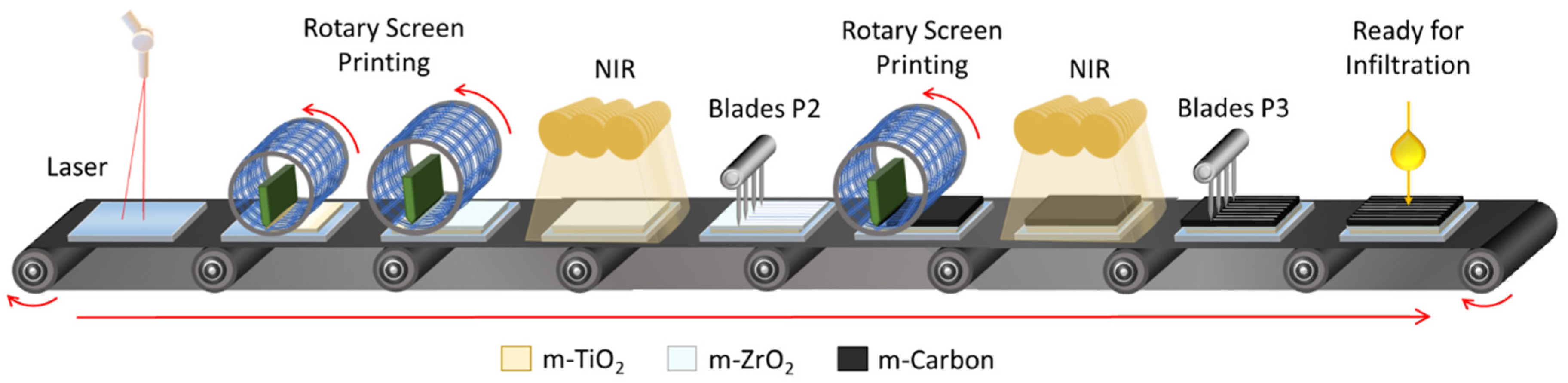
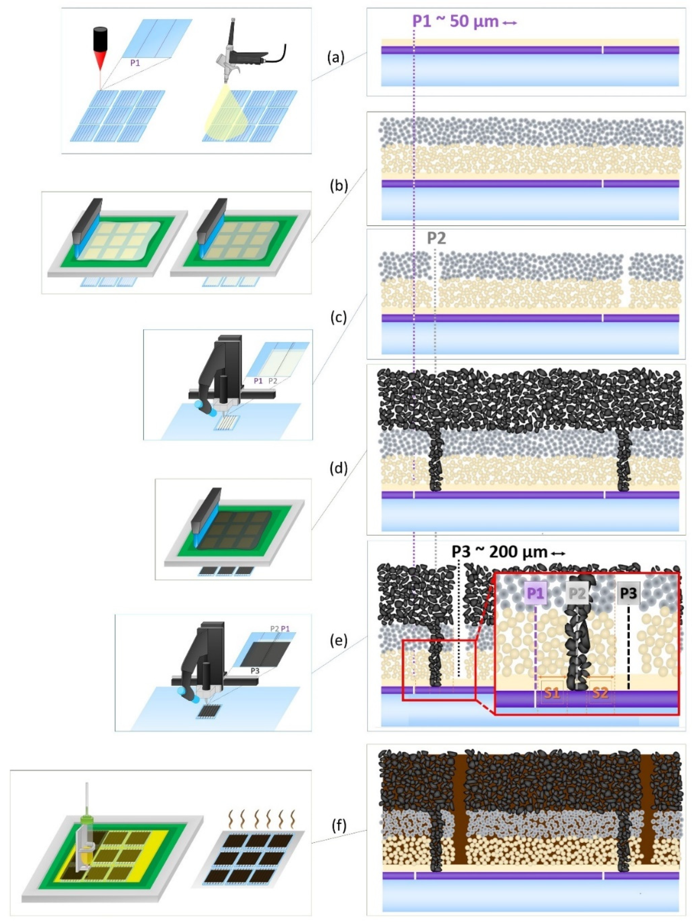
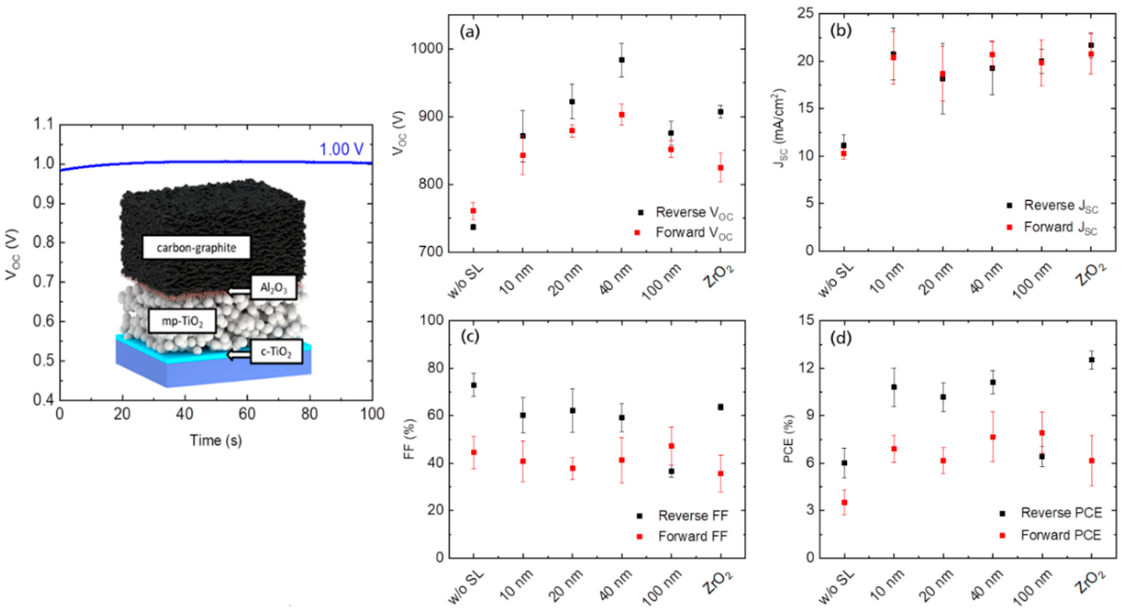
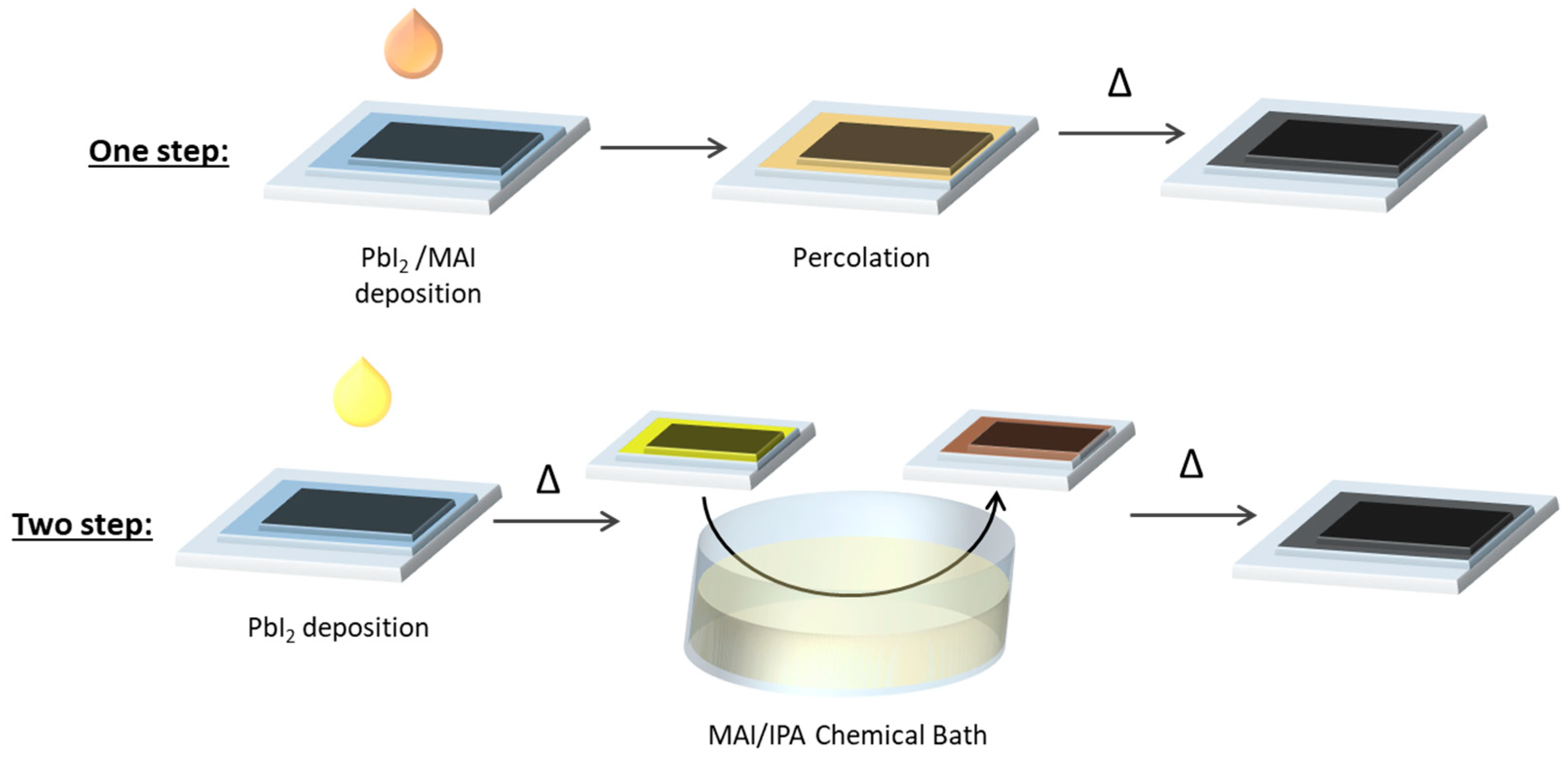
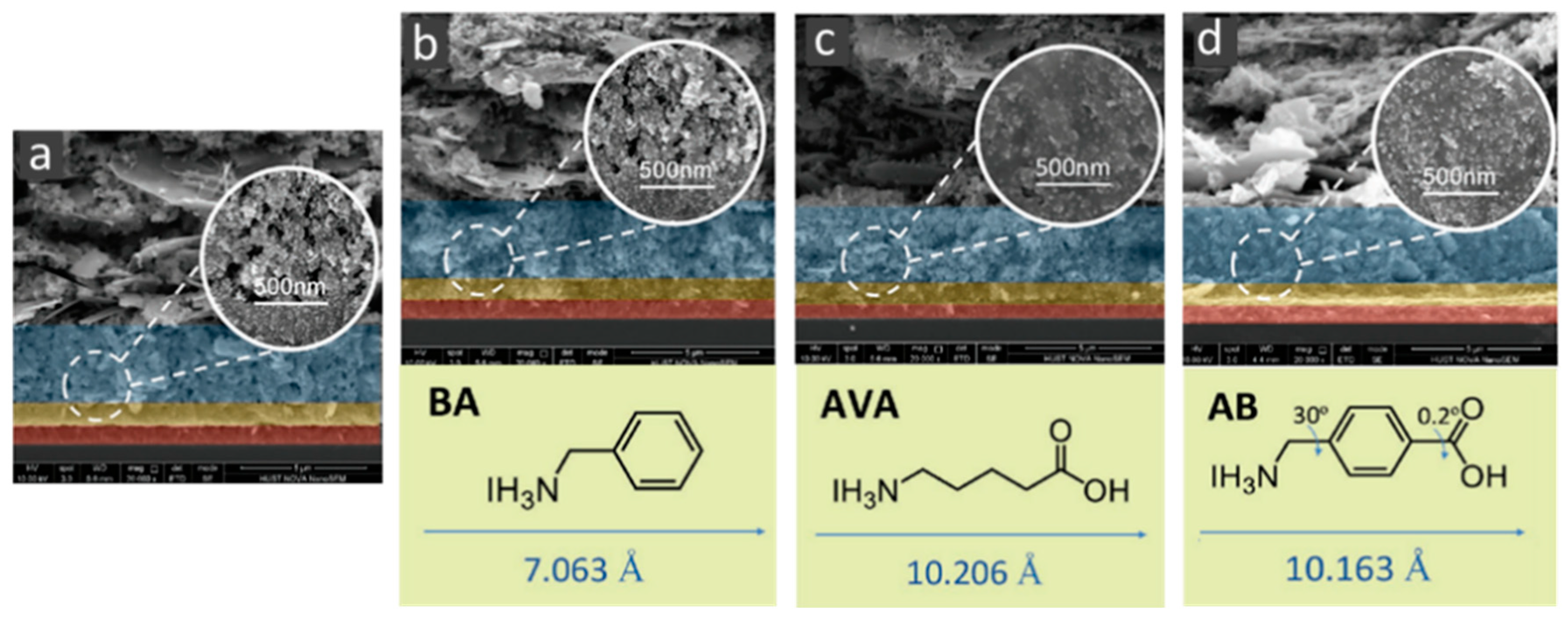
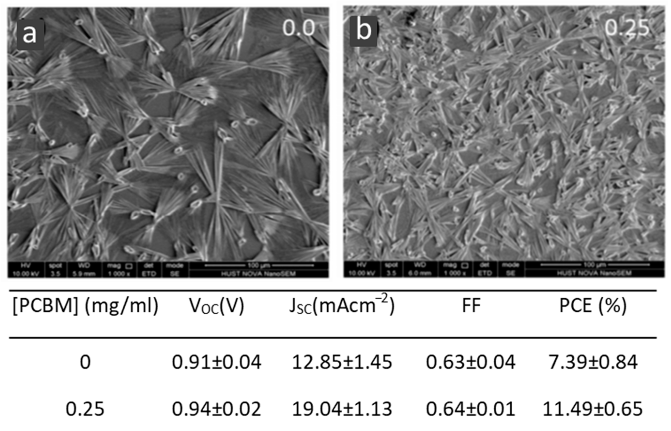
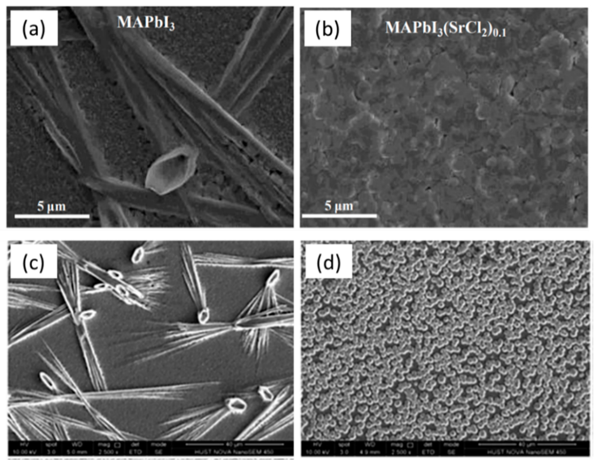
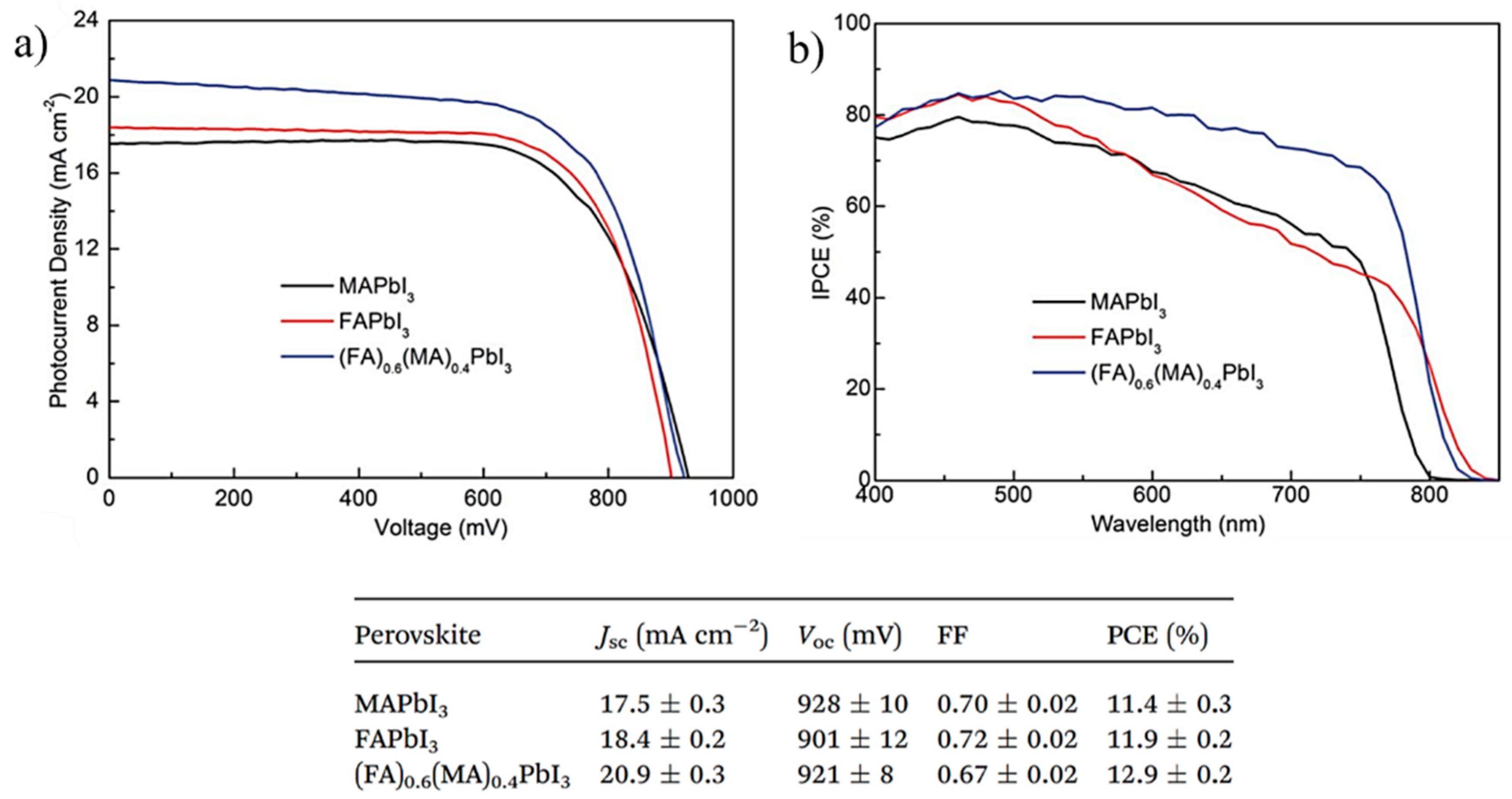
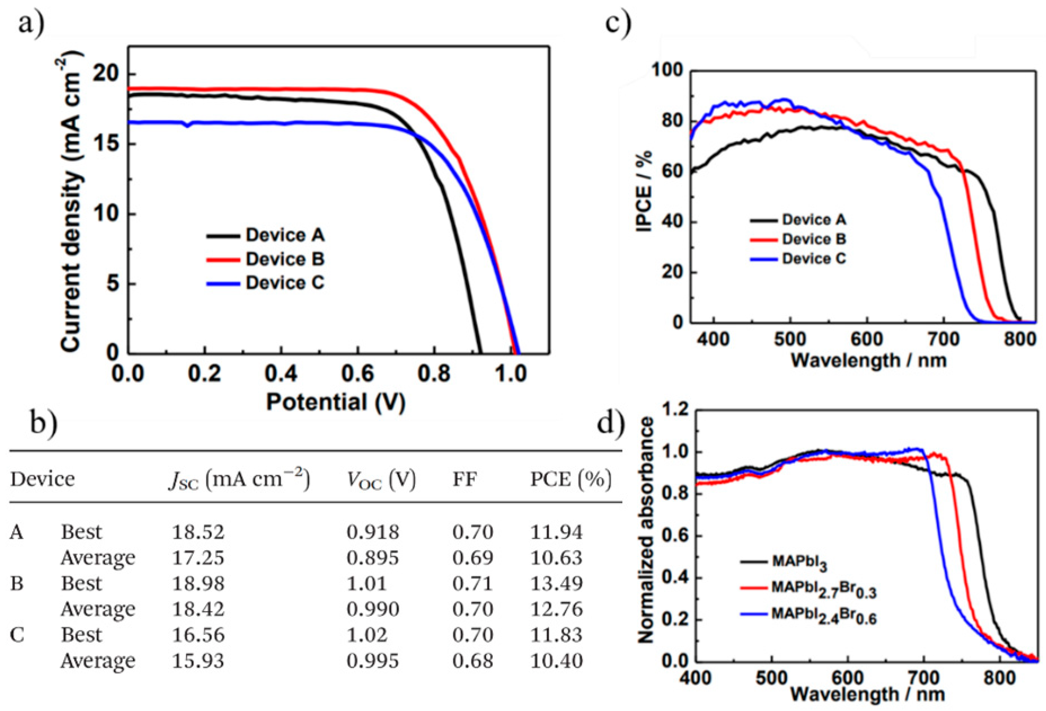
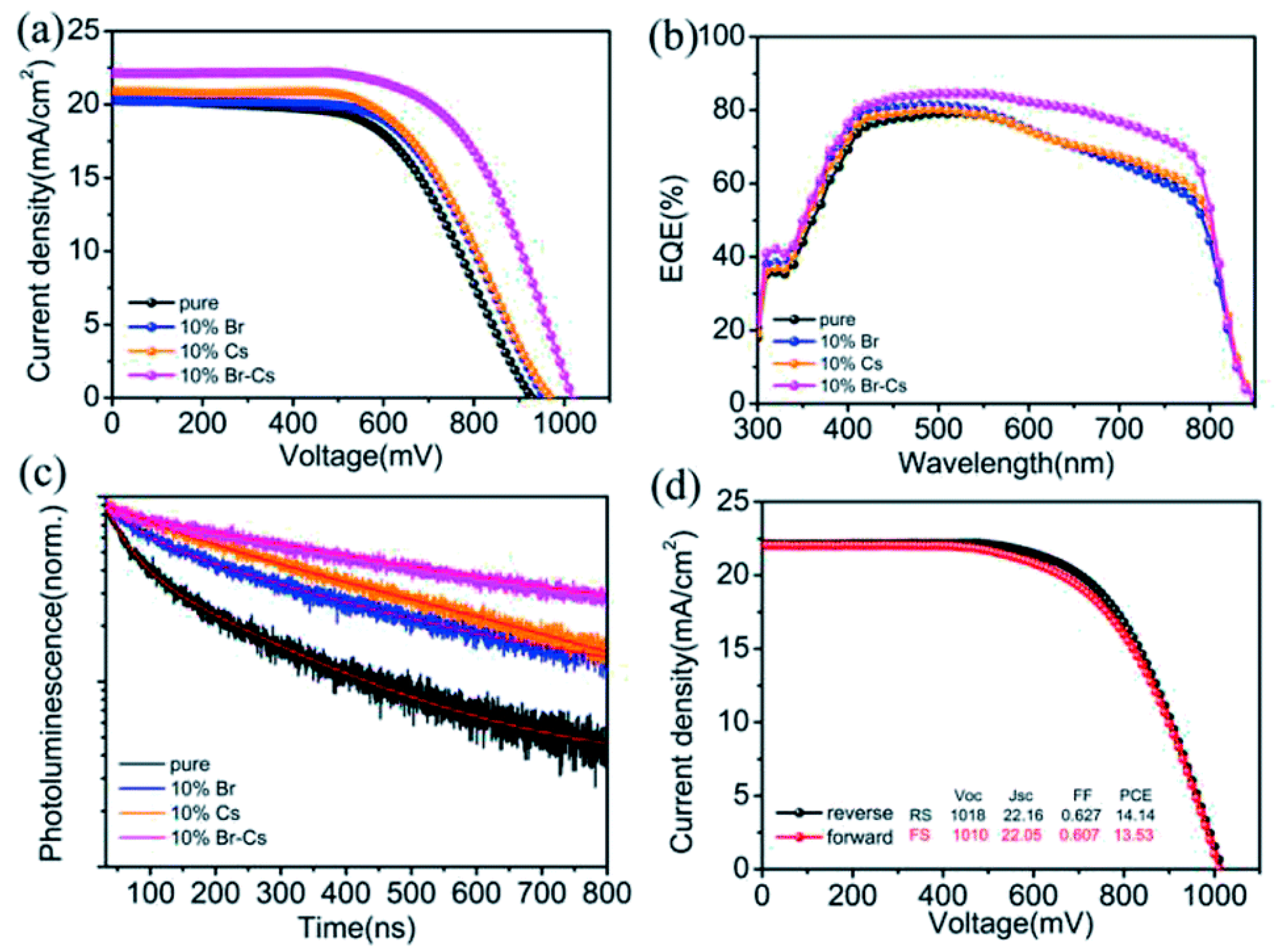
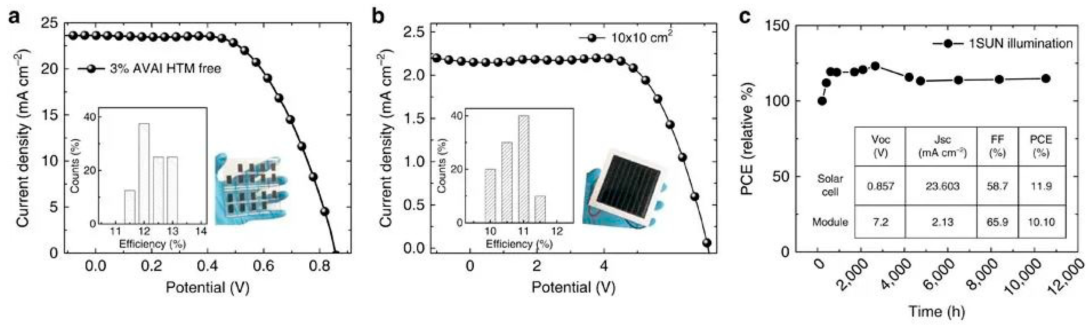
Table 1.
Summary of reported with information about materials, processing and PCE values. All the devices were prepared on FTO glass (F:SnO2). Film deposition methods are: (1) spray pyrolysis, (2) screen-printing, (3) spin coating, (4) sputtering, (5) vacuum evaporation, (6) doctor-blade, (7) inkjet. Infiltration methods: (a) drop casting, (b) spin coating, (c) Inkjet, (d) RbM. Only optimal performance is reported. When a range of thickness is reported, the table refer to an average value.
| Ref | Inorganic Stack Materials, Deposition Method and Thickness | Perovskite Formulation | PCE (%) Illumination Area (mm2), Publication Year | Voc (mV) Jsc (mA/cm2) FF (%) | Comments |
|---|---|---|---|---|---|
| [14] | TiO2(1)(100 nm)/TiO2(2)(1 µm)/ ZrO2(2)(1 µm)/C(2)(10 µm) | MAPbI3, one step(a) | 6.64 (12.5) 2013 | 878/12.4/61 | First report on mCPSC |
| [12] | TiO2(1)/TiO2(2)(0.6 µm)/ ZrO2(2)(1 µm)/C(2)(10 µm) | MAPbI3, two steps(b) | 10.64 (13) 2014 | 868/20.1/61 | TiO2 in nano-sheets |
| [25] | TiO2(1)/TiO2(2)(1 µm)/ ZrO2(2)(2 µm)/C(2)(10 µm) | AVA-MAPbI3, one step(a) | 11.6 (7) 2014 | 843/21.1/65 | First report on AVA-MAPbI3 |
| [70] | TiO2(1)/TiO2(2)(0.4 µm)/ ZrO2(2)(0.5 µm)/C(2)(9 µm) | MAPbI3, two steps(a) | 11.6 2014 | 894/18.1/72 | |
| [69] | TiO2(1)(100 nm)/TiO2(2)(1 µm)/ ZrO2(2)(1 µm)/C(2)(5 µm) | MAPbI3, one step(a) | 7.08 (13) 2015 | 867/15.2/54 | |
| [52] | TiO2(1)/TiO2(2)/ZrO2(2)/C(2) | MAPbI3, either one or two steps(a) | 12.3 2015 | 921/18.3/73 | |
| [63] | TiO2(1)/TiO2(2)(0.4 µm)/ Al2O3(2)(0.4 µm)/NiO(2)(0.8 µm)/C(6)(10 µm) | MAPbI3, two steps(a) | 15.0 (16) 2015 | 915/21.6/76 | First mCPSC with NiO interlayer |
| [80] | TiO2/TiO2(7)/ZrO2(7)/NiO(7)/C(7) | MAPbI3, two steps | 14.9 2015 | 917/21.4/76 | |
| [76] | TiO2(1)/TiO2(2)(0.4 µm)/ Al2O3(2)(0.65 µm)/C(2)(10 µm) | MAPbI3, two steps(a) | 14.7 (19.6) 2016 | 1010/21.3/69 | SWCNT in the carbon electrode |
| [15] | TiO2(1)(50 nm)/TiO2(2)(0.6 µm)/ ZrO2(2)(1.5 µm)/C(2)(8 µm) | MAPbI3, two steps(a) | 11.3 (6.5) 2017 | 780/21.9/66 | NIR-fast annealing for the inorganic stack |
| [58] | TiO2/TiO2(2)/Al2O3(2)/NiO(2)/C(2) | Csx(FA0.4MA0.6)1-x PbI2.8Br0.2, two step(a) | 17.02 (12.9) 2017 | 1008/23.4/72 | Highest performance so far |
| [34] | TiO2(1)(35 nm)/TiO2(2)(0.5 µm)/ ZrO2(2)(2 µm)/C(2) | AVA-MAPbI3, one step(c) | 9.53 (16) 2017 | 861/16.6/67 | Inkjet to infiltrate the perovskite solution |
| [71] | TiO2(1)/TiO2(2)/ZrO2(2)/C(2) | AVA-MAPbI3, one step(a) | 14.1 2017 | 901/23.0/68 | Use of ultra-thin graphite |
| [75] | TiO2(1)/TiO2(2)/ZrO2(2)/C(2) | AVA-MAPbI3, one step(a) | 13.6 2017 | 940/22.9/63 | Boron-doped graphite |
| [64] | TiO2(1)(50 nm)/TiO2(2)(0.45 µm)/ Al2O3(2)(0.9 µm)/NiO-SWCNT (2)(1.8 µm) | MAPbI3, two steps(a) | 12.7 (20) 2017 | 945/20.7/64 | NiO/SWCNT composite as top electrode |
| [46] | TiO2(2)/ZrO2(2)(2.1 µm)/C(2)(13 µm) | AVA-MAPbI3, one step(a) | 9.11 2017 | 880/23.5/44 | Double mesoscopic stack |
| [81] | TiO2(1)(50 nm)/TiO2(2)/ Al2O3(0.45 µm)(2)/NiOx (2)/C(2)(5 µm) | MAPbI3, two steps(a) | 11.3 2017 | 945/17.2/69 | O3 treatment on to oxidise Ni2+→Ni3+ for NiOx layer |
| [36] | TiO2(1)/TiO2(2)/ZrO2(2)/C(2) | MAPbI3, two steps(d) | 10.4 (9) 2018 | 802/19.9/65 | RbM deposition for PbI2 |
| [74] | TiO2(1)/TiO2(2)(0.8 µm)/ ZrO2(2)(1.2 µm)/C(2)(10 µm) | AVA-MAPbI3, one step(a) | 15.7 2018 | 980/23.2/69 | Oxygen-rich carbon electrode |
| [53] | TiO2(1)/TiO2(2)(0.5 µm)/ ZrO2(2)/C(2)(10µm)/c-C(2)(20 µm) | AVA-MAPbI3, one step(a) | 13.9 (10.2) 2018 | 920/23.4/65 | Compact carbon layer with p-type doping on the top |
| [54] | TiO2(1)/TiO2(2)(0.5 µm)/Al2O3(1)(<2.4 nm) ZrO2(2)(1.2 µm)/C(2)(15 µm) | AVA-MAPbI3, one step(a) | 14.4 (10.8) 2018 | 900/22.8/70 | |
| [61] | TiO2(1)/TiO2(2)/Al2O3(5)(10 nm)/ ZrO2(2)(1 µm)/C(2) | AVA-MAPbI3, one step(a) | 14.3 (10.7) 2018 | 930/23.3/66 | |
| [68] | TiO2(3)/TiO2(3)/SiO2(3)/C(6) | AVA-MAPbI3, one step(a) | 13.1 2018 | 900/22.6/64 | |
| [82] | TiO2(2)/TiO2(2)/ZrO2(2)/Co3O4(2)(70 nm)/C(2) | AVA-MAPbI3, one step(a) | 13.3 (9) 2018 | 880/23.4/64 | |
| [37] | TiO2(2)(50 nm)/TiO2(2)(0.5 µm)/ZrO2(2) (1.4 µm)/Cu:NiOx(2)(80 nm)/C(2)(13 µm) | AVA-MAPbI3, one step(a) | 12.79 (80) 2019 | 1000/22.2/57 | 12.1% on 70 cm2 module |
| [21] | TiO2/TiO2(2)/ZrO2(2)/C(2)(12 µm) | AVA-MAPbI3, one step(a) | 13.3 (16.0) 2019 | 900/21.4/69 | |
| [78] | TiO2(3)/TiO2(3)/Al2O3(3)/C(2) | AVA-MAPbI3, one step(a,b) | 10.8 (30) 2019 | 934/18.0/64 | WO3 in the carbon layer |
| [55] | TiO2(1)(50 nm)/TiO2(2)(1µm)/ZrO2(2)/ C(2)(15 µm) | AVA-MAPbI3, one step(a) | 11.9 (13) 2019 | 871/19.1/71 | Optimisation of the ZrO2 layer |
| [59] | TiO2(1)/TiO2(2)(1 µm)/Al2O3(2)(1.2 µm)/ C(2)(15 µm) | MAPbI3, two steps(b) | 10.7 (16) 2019 | 870/19.3/64 | In presence of water |
| [47] | TiO2(3)/TiO2(2)/ZrO2(2)/C(2) | AVA-MAPbI3, one step(a) | 10.81 (10) 2019 | 910/19.1/62 | Dual-sized TiO2 particles |
| [79] | TiO2(1)/TiO2(2)(0.45 µm)/ZrO2(2)(0.4 µm)/ NiO(2)(1 µm)/C(2)(8 µm) | MAPbI3, two steps(a) | 14.2 2019 | 965/20.4/72 | Use of NiO nanosheets |
| [83] | TiO2/TiO2/ZrO2/C | AVA-MAPbI3, one step(a) | 14.6 (16) 2019 | 891/21.9/75 | CuSCN in the perovskite formulation |
| [73] | TiO2(3)/TiO2(2)(450 nm)/ ZrO2(2)(1.7 µm)/C(2)(25 µm) | AVA-MAPbI3, one step(a) | 10.0 (10) 2019 | 890/21.7/52 | Spiro-OMeTAD spin coated on the top |
| [72] | TiO2(1)(50 nm)/TiO2(2)(0.6 µm)/ ZrO2(2)(1.5 µm)/C(2)(13 µm) | AVA-MAPbI3, one step(a) | 13.2 (49) 2020 | 810/23.8/68 | Laminated Cu-grid |
| [57] | TiO2(1)/TiO2(2)(0.5 µm)/ ZrO2(2)(0.75 µm)/C(2)(15 µm) | Cs0.1Rb0.05FA0.85PbI3, one step(a) | 16.2 (10.8) 2020 | 909/22.7/79 | |
| [60] | TiO2(4)(20 nm)/TiO2(2)(1.5 µm)/ Al2O3(4)(40 nm)/C(2)(8 µm) | AVA-MAPbI3, one step(a) | 11.1 (40) 2020 | 983/19.3/59 | Very thin spacer layer |
| [48] | TiO2(3)/TiO2+EuW10(2)/ZrO2(2)/C(2) | AVA-MAPbI3, one step(a) | 14.36 (10) 2020 | 880/23.5/72 | Optimisation of the EuW10:TiO2 ratio |
| [35] | TiO2(7)/TiO2(7)/ZrO2(7)/C(2) | AVA-MAPbI3, one step(c) | 9.1 (64) 2020 | 900/17.2/59 |
Table 2.
Summary of reported mCPSCs, with information about materials, processing and PCE values. All the devices were prepared on FTO glass. Deposition methods are mentioned with the following notes: (1) spray pyrolisis, (2) screen-printing, (3) spin coating, (4) chemical bath deposition (5) doctor blading. Infiltration methods are mentioned with the following notes: (a) drop casting. The best performing devices from each article are listed here. When a range of thickness is reported, the table refers to an average value. where two references are reported, the associated works include the first example of a given perovskite in mCPSCs and the publication presenting the current highest PCE for that formulation.
| Ref | Inorganic Stack Materials, Deposition Method and Thickness | Perovskite Formulation | PCE (%) Illumination Area (mm2), Publication Year | Voc (mV) Jsc (mA/cm2) FF (%) | Comments |
|---|---|---|---|---|---|
| [147] | TiO2(1)/TiO2(2)(0.4 µm)/ ZrO2(2)(1.5 µm)/C(2)(10 µm) | MAPbI3, one-step(a), DMF | 10.5(7) 2016 | 914, 16.92, 68 | |
| [127] | TiO2(1)/TiO2(2)(0.4 µm)/ Al2O3 (2)(0.5 µm)/C(2)(8 µm) | MAPbI3, one-step(a), DMF | 13(16) 2017 | 950, 19.5, 70 | |
| [94,148] | TiO2(1)(0.1 µm)/TiO2(2)(0.7 µm)/ZrO2(2)(1.5 µm)/C(2)(10 µm) | MAPbI3, two-step, DMF, IPA | 11.4(7) 2014 | 928, 17.5, 70 | Average cell values |
| [111] | TiO2(1)/TiO2(2)(1 µm)/ Al2O3 (2)(1 µm)/C(2)(10 µm) | MAPbI3, one-step(a), NMP | 15(9) 2017 | 893, 22.43, 75 | Highly controlled solvent vapour environment |
| [14] | TiO2(1)/TiO2(2)(1 µm)/ ZrO2(2)-(1 µm)/C(2)(10 µm) | MAPbI3, one-step(a), GBL | 6.6(12.5) 2013 | 878, 12.4, 61 | With Spheroidal graphite |
| [38,83] | TiO2(1)/TiO2(2)-(0.5 µm)/ ZrO2(2)(1.5 µm)/C(2)(20 µm) | AVAxMA(1-x)PbI3, one-step(a), GBL | 15.3(16) 2019 | 869, 21.2, 83 | 30 min ambient infiltration time, 5 day humidity treatment |
| [110] | TiO2(1)/TiO2(2)(0.5 µm)/ ZrO2(2)(3 µm)/C(2)(10 µms) | AVAxMA(1-x)PbI3, one-step(a), GBL/Ethanol | 15.1(10) 2019 | 900, 23.58, 71 | |
| [99] | TiO2(3)/TiO2(3)(0.5 µm)/ ZrO2(3)(1.5 µm)/C(3)(13 µm) | AVAxMA(1-x)PbI3, one-step, DMF | 9.1 2020 | 848, 23.8, 45 | |
| [101] | TiO2(1)/TiO2(3)(2 µm)/ ZrO2(2)(1.8 µm)/C(5)(24 µm) | AVAxMA(1-x)PbI3.PEAI one-step | 6.72 2020 | 875, 15.8, 49 | Extremely thick TiO2 |
| [83] | TiO2(1)/TiO2(2)(1 µm)/ ZrO2(2)(2.2 µm)/C(2)(20 µm) | AVAxMA(1-x)PbI3, 0.04 CuSCN, one-step, GBL | 15(16) 2019 | 888, 21.9, 77 | 30 min ambient infiltration time, 5 day humidity treatment |
| [99] | TiO2(4)/TiO2(3)(0.5 µm)/ ZrO2(3)(1.5 µm)/C(3)(13 µm) | (Leucine)xMA(1-x)PbI3, one-step(a), DMF | 9.0 2020 | 838, 24.2, 45 | |
| [98] | TiO2(1)/TiO2(2)(0.5 µm)/ ZrO2(2)(2 µm)/C(2)(15 µm) | ABxMA(1-x)PbI3, one-step(a), GBL | 15.6(12.6) 2018 | 940, 23.4, 71 | |
| [149] | TiO2(1)/TiO2(2)(0.5 µm)/ ZrO2(2)(2 µm)/C(2)(15 µm) | MAPbI3, 2% MLAI, one-step, DMF/DMSO 4:1 | 13.86(10) 2020 | 940, 20.34, 72 | |
| [100] | TiO2(1)/TiO2(2)/ZrO2(2)/C(2) | MAPbI3.0.15CH4N2S, one-step(a), DMF | 13.0 2019 | 910, 22.39, 64 | |
| [148] | TiO2(1)/TiO2(2)(0.6 µm)/ ZrO2(2)(2.5µm)/C(2)(12 µm) | AVA0.034MA0.9PbI2.95(BF4)0.05 one-step(a), GBL | 15.5(10) 2018 | 970, 24.37, 66 | |
| [104,147] | TiO2(1)/TiO2(2)(0.4 µm)/ ZrO2(2)(1.5 µm)/C(2)(10 µm) | MAPbI2.95(BF4)0.05, one-step(a), DMF | 13.24(7) 2016 | 957, 18.15, 76 | |
| [134] | TiO2(1)/TiO2(2)(0.5 µm)/ ZrO2(2)(1.4 µm)/C(2)(10 µm) | CsAVA0.05MA0.95PbI3, one-step, GBL | 12.2(14.8) 2018 | 893, 20.59, 66 | High annealing temp. (100 °C, 1 h) |
| [118] | TiO2(1)/TiO2(2)(1 µm)/ ZrO2(2)(1.6 µm)/C(2)(11 µm) | MAPbI3.0.45MACl, one-step, DMF | 14.5(14.8) 2018 | 1033, 20.14, 70 | High annealing temp. (100 °C, 20 min) |
| [102] | TiO2(1)/TiO2(2)(0.5 µm)/ ZrO2(2)(0.5 µm)/C(2)(10 µm) | MAPbI3.0.25GuCl, one-step(a), DMF | 14.35(12.6) 2017 | 1000, 19.31, 74 | |
| [105] | TiO2(3)/TiO2(2)(1.4 µm)/ ZrO2(2)(1.4 µm)/C(2) | MAPbI3.0.1CQD, one-step(a), DMF | 7.62 2018 | 790, 16.4, 62 | With TiO2 nanosheets |
| [104] | TiO2(1)/TiO2(2)(0.6 µm)/ ZrO2(2)(2 µm)/C(2)(12 µm) | MAPbI3, 25mg/mL PCBM one-step(a), DMF | 12.36 2018 | 930, 20.26, 66 | High annealing temp. (100 °C, 5 min) |
| [104] | TiO2(1)/TiO2(2)(0.6 µm)/ ZrO2(2)(2 µm)/C(2)(12 µm) | MAPbI2.95(BF4)0.05, 25mg/mL PCBM, one-step(a), DMF | 14.26 2018 | 990, 20.55, 70 | High annealing temp., (100 °C, 5 min) |
| [113] | TiO2(1)/TiO2(2)(1 µm)/ ZrO2(2)(1 µm)/C(2)(10 µm) | MAPbI3, 53.3mg/mL NH4Cl, one-step, DMF | 15.6(12.6) 2017 | 940, 21.45, 77 | With humidity exposure |
| [126] | TiO2(1)/TiO2(2)(0.5 µm)/ ZrO2(2)(2 µm)/C(2)(10 µm) | MAPbI3.0.3LiCl, one-step (a), DMF | 14.5(10) 2016 | 927, 20.2, 77 | High annealing temp. (100 °C, 10 min) |
| [127] | TiO2(1)/TiO2(2)(0.4 µm)/ Al2O3 (2)(0.5 µm)/C(2)(8 µm) | MAPbI3.0.1SrCl2, one-step(a), DMF | 15.9(16) 2017 | 1050, 20.15, 75 | |
| [94] | TiO2(1)(0.1 µm)/TiO2(2)(0.7 µm)/ZrO2(2)(1.5 µm)/C(2)(10 µm) | FAPbI3, two-Step, DMF, IPA | 11.9(7) 2014 | 901, 18.4, 72 | |
| [94] | TiO2(1)(0.1 µm)/TiO2(2)(0.7 µm)/ZrO2(2)(1.5 µm)/C(2)(10 µm) | FA0.4MA0.6PbI3, two-step, DMF, IPA | 12.9(7) 2014 | 921, 10.9, 67 | |
| [58] | TiO2(1)/TiO2(2)(0.46 µm)/ Al2O3(2) (0.45 µm)/ NiO(2)(0.8 µm)/C(2)(10 µm) | FA0.4MA0.6PbI2.8Br0.2 | 14.88(12.9) 2017 | 953, 22.31, 70 | NiO hole extraction layer present |
| [58] | TiO2(1)/TiO2(2)-(0.46 µm)/ Al2O3(2)(0.45 µm)/ NiO(2)(0.8 µm)/C(2)(10 µm) | Cs0.05(FA0.4MA0.6)0.95 PbI2.8Br0.2, two-step, DMF, IPA | 17(12.9) 2017 | 1008, 23.4, 72 | NiO hole extraction layer present |
| [90] | TiO2(1)(0.1 µm)/TiO2(2)(1 µm)/ ZrO2(2)(2 µm)/C(2)(10 µm) | Cs0.1FA0.9PbI3, one-step, DMF/DMSO | 15(10) 2019 | 920, 23.63, 69 | Solvent vapour assisted crystallisation. |
| [89] | TiO2(1)(0.1 µm)/TiO2(2)(1 µm)/ ZrO2(2)(1.5 µm)/C(2)(10 µm) | Cs0.1FA0.9PbI3, two-step, DMF, IPA | 11.72(14.8) 2019 | 970, 20.91, 58 | |
| [89] | TiO2(1)(0.1 µm)/TiO2(2)(1 µm)/ ZrO2(2)(1.5 µm)/C(2)(10 µm) | FAPbI2.9Br0.1, two-step, DMF, IPA | 11.53(14.8) 2019 | 950, 20.29. 59 | |
| [89] | TiO2(1)(0.1 µm)/TiO2(2)(1 µm)/ ZrO2(2)(1.5 µm)/C(2)(10 µm) | Cs0.1FA0.9PbI0.9Br0.1, two-step, DMF, IPA | 14.14(14.8) 2019 | 1018, 22.16, 63 | |
| [57] | TiO2(1)(0.1 µm)/TiO2(2)(0.5 µm)/ZrO2(2)(0.75 µm)/C(2)(15 µm) | Cs0.1Rb0.05FA0.85PbI3, one-step, DMF/DMSO/5% Formamide | 16.21(10.8) 2019 | 909, 22.69, 79 | 2 h solvent vapour assisted crystallisation. |
| [57] | TiO2(1)(0.1 µm)/TiO2(2)(0.5 µm)/ZrO2(2)(0.75 µm)/C(2)(15 µm) | Cs0.1Rb0.05FA0.85PbI3, one step, DMF/DMSO | 14.59(10.8) 2019 | 888, 22.56, 72 | 2 h solvent vapour assisted crystallisation Average device values. |
| [57] | TiO2(1)(0.1 µm)/TiO2(2)(0.5 µm)/ZrO2(2)(0.75 µm)/C(2)(15 µm) | Cs0.1Rb0.05FA0.85PbI3, one-step, DMF | 6.42(10.8) 2019 | 867, 11.12, 66 | 2 h solvent vapour assisted crystallisation. Average device values. |
| [141] | TiO2(1)/TiO2(2)(0.4 µm)/ Al2O3 (2)(1.2 µm)/C(2)(10 µm) | MAPbI2.7Br0.03, two-step, DMF, IPA | 13.49 2016 | 1010, 18.93, 71 | |
| [142] | TiO2(1)/TiO2(2)(0.4 µm)/ Al2O3 (2)(0.6 µm)/C(2)(10 µm) | MAPbI2Br, two-step, DMF, IPA | 11.03(16) 2015 | 1040, 15.37, 69 |
Table 3.
Some of the most stable perovskite devices with their configurations, PCEs, stability times and test conditions. In gray, the highest stability for mCPSCs. Adopted from reference [156].
Table 3.
Some of the most stable perovskite devices with their configurations, PCEs, stability times and test conditions. In gray, the highest stability for mCPSCs. Adopted from reference [156].
| Ref. | Architecture | Test Conditions | PCE (%) | PCE Loss (%) | Stability Time |
|---|---|---|---|---|---|
| [157] | FTO/TiO2-Cl/MAPbI3/Spiro/Au | Unsealed, stored in dark, RH < 30%. | 21 | 4 | 2000 h |
| [158] | FTO/doped C60/mixed perovskite/spiro/Au | Exposed to air, RH ~55% | 17.6 | 20 | 650 h |
| [159] | ITO/PEDOT:PSS/MAPbI3/PCBM/EFGnPs-F/Al | Exposed to air, RH ~50% | 14.3 | ~10 | 30 days |
| [160] | FTO/LBSO/MAPbI3/PTAA/Au | In N2, at 25 °C, illuminated with UV component | 21.2 | <10 | 120 h |
| [27] | FTO/TiO2/TiO2/perovskite (3% AVAI)/ZrO2/Carbon | sealed under an ambient environment, 55 °C, constant illumination without UV component | 11.9 | none | 10,000 h |
| [28] | FTO/TiO2/TiO2/AVA-MAPbI3/ZrO2/Carbon | maximum power point of 55 °C ± 5 °C, following the IEC61215:2016 Standards | none | 9000 h | |
| [160] | ITO/TiO2/TiO2/perovskite/PTAA/Au | In N2, high temp. and illumination | 20.6 | 10 | 160 h |
| [161] | FTO/TiO2/TiO2/mixed perovskite/Spiro-OMeTAD-SWCNT | N2 atmosphere, LED white light equivalent to 1 Sun, and at 60 °C | 15 | 20 | 580 h |
Publisher’s Note: MDPI stays neutral with regard to jurisdictional claims in published maps and institutional affiliations. |
© 2021 by the authors. Licensee MDPI, Basel, Switzerland. This article is an open access article distributed under the terms and conditions of the Creative Commons Attribution (CC BY) license (http://creativecommons.org/licenses/by/4.0/).
Share and Cite
MDPI and ACS Style
Meroni, S.M.P.; Worsley, C.; Raptis, D.; Watson, T.M. Triple-Mesoscopic Carbon Perovskite Solar Cells: Materials, Processing and Applications. Energies 2021, 14, 386. https://doi.org/10.3390/en14020386
AMA Style
Meroni SMP, Worsley C, Raptis D, Watson TM. Triple-Mesoscopic Carbon Perovskite Solar Cells: Materials, Processing and Applications. Energies. 2021; 14(2):386. https://doi.org/10.3390/en14020386
Chicago/Turabian StyleMeroni, Simone M. P., Carys Worsley, Dimitrios Raptis, and Trystan M. Watson. 2021. "Triple-Mesoscopic Carbon Perovskite Solar Cells: Materials, Processing and Applications" Energies 14, no. 2: 386. https://doi.org/10.3390/en14020386
Note that from the first issue of 2016, this journal uses article numbers instead of page numbers. See further details here.